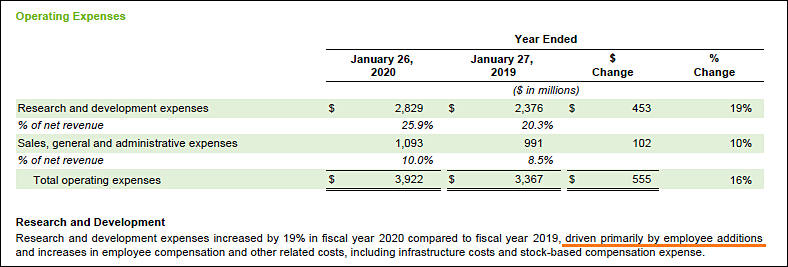
-
Lakefield chip
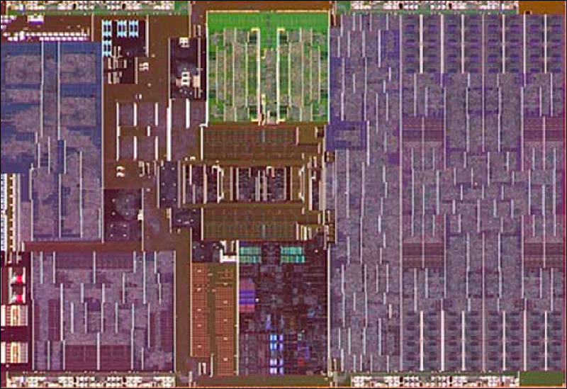
4x Atom (green) + 1x Core (dark area at bottom center) + GPU (right ~40%) + uncore (left ~30%)
 sa12495.jpg800 x 549 - 100K
 -
Intel’s options include stopping operating its own NAND foundry and buying in chips, or even sourcing complete SSDs from a third party. Alternatively, it could sell chips to third parties.
Intel need to sale parts to stay afloat, this is why such talks began.
-
TSMC is set to kick off volume production of chips built using 5nm process technology in April, and has already seen the process capacity fully booked by clients, according to industry sources.
-
It turns out that the next step to TSMC N7, the company's current-generation 7 nm DUV silicon fabrication node, isn't N7+ (7 nm EUV), but rather it has a nodelet along the way, which the foundry refers to as N7P. This is a generational refinement of N7, but does not use EUV lithography, which means it may not offer the 15-20 percent gains in transistor densities offered by N7+ over N7.
AMD clarified that "7 nm+" in its past presentations did not intend to signify N7+, and that the "+" merely denoted an improvement over N7.
Bad days of TSMC.
-
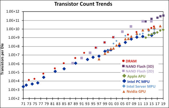
Power consumption and challenges associated with scaling limitations have cut into the transistor growth rates of some IC products during the last 10-15 years. DRAM transistor counts were increasing at the average rate of about 45% per year through the early 2000s but slowed to about 20% through the 16Gb generation that appeared in 2016. Samsung began volume production with single-chip 16Gb DRAM devices near the end of 2016. One year earlier Samsung initiated volume production of 12Gb DRAM chips, and 8Gb devices one year before that. The DDR5 standard still being finalized by JEDEC includes monolithic 24Gb, 32Gb, and 64Gb devices.
Annual growth in flash memory densities remained at 55-60% per year through about 2012 but has since been around 30-35% per year. For conventional 2D planar NAND flash, the highest density on a single die available in January 2020 was 128Gb. The maximum density for a 3D NAND chip is currently 1.33Tb for a 96-layer quad-level-cell (QLC) device. QLC combined with new 96-layer technology should enable 3D NAND to reach 1.5Tb density in 2020 with 128-layer technology leading to 2Tb chips.
Transistor counts in Intel’s PC microprocessors grew approximately 40% per year through 2010, but the rate dropped to half that in the years following. Transistor count increases for the company’s server MPUs paused in the mid- to late-2000s but then started growing again at the rate of about 25% per year. Intel stopped revealing details of transistor counts in 2017.
Transistor counts for Apple’s A series application processors used in its iPhones and iPads have increased at the annual rate of 43% since 2013. That rate includes as the most recent endpoint the A13 processor, with its 8.5 billion transistors. In the first half of 2020, Apple is expected to unveil an iPad Pro based on a new A13X processor.
 sa12455.jpg590 x 377 - 41K
 -
AMD also won't use 7nm+ EUV process for Zen 3, as it seems like it is not ready at all
Same is true for their GPUs.
Sad news for TSMC, while marketing "5nm" can work, they can be last process before long pause similar to Intel one.
Early leaks talk about only 3-5% speed improvement assisted with 10-15% price hike.
 sa12441.jpg746 x 417 - 37K
 -
AMD Finances

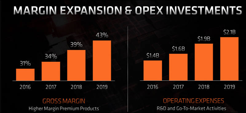
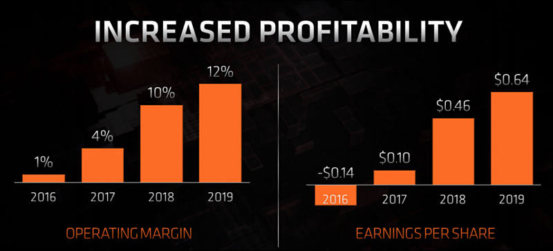
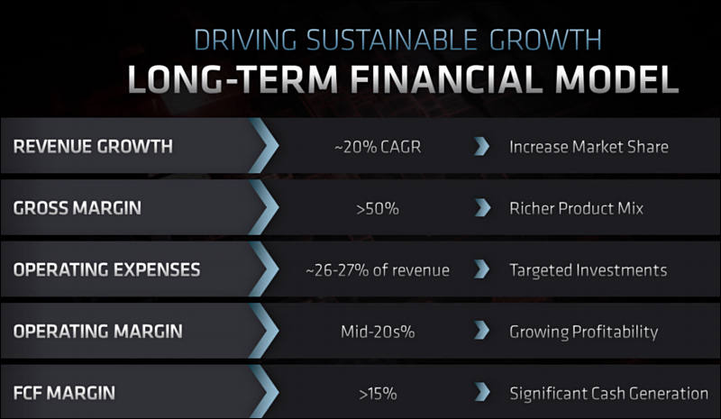
Short summary - more marketing expenses, more profits for shareholders, much more expensive CPUs for consumers.
 sa12434.jpg800 x 449 - 37K
 sa12435.jpg800 x 369 - 38K
 sa12436.jpg800 x 363 - 33K
 sa12437.jpg800 x 465 - 45K
 -
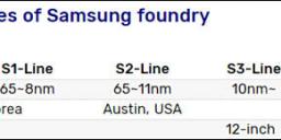
Samsung Electronics, a world leader in advanced semiconductor technology, today announced that its new cutting-edge semiconductor fabrication line in Hwaseong, Korea, has begun mass production.
This is Samsung’s first semiconductor production line dedicated to the extreme ultraviolet (EUV) lithography technology and produces chips using process node of 7 nanometer (nm) and below. The V1 line broke ground in February 2018, and began test wafer production in the second half of 2019. Its first products will be delivered to customers in the first quarter.
The V1 line is currently producing state-of-the-art mobile chips with 7 and 6nm process technology and will continue to adopt finer circuitry up to the 3nm process node.
By the end of 2020, the cumulative total investment in the V1 line will reach USD 6 billion in accordance with Samsung’s plan and the total capacity from 7nm and below process node is expected to triple from that of 2019. Together with the S3 line, the V1 line is expected to play a pivotal role in responding to fast-growing global market demand for single-digit node foundry technologies.
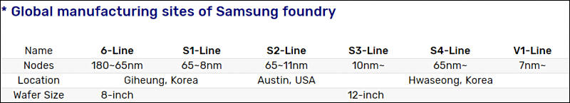
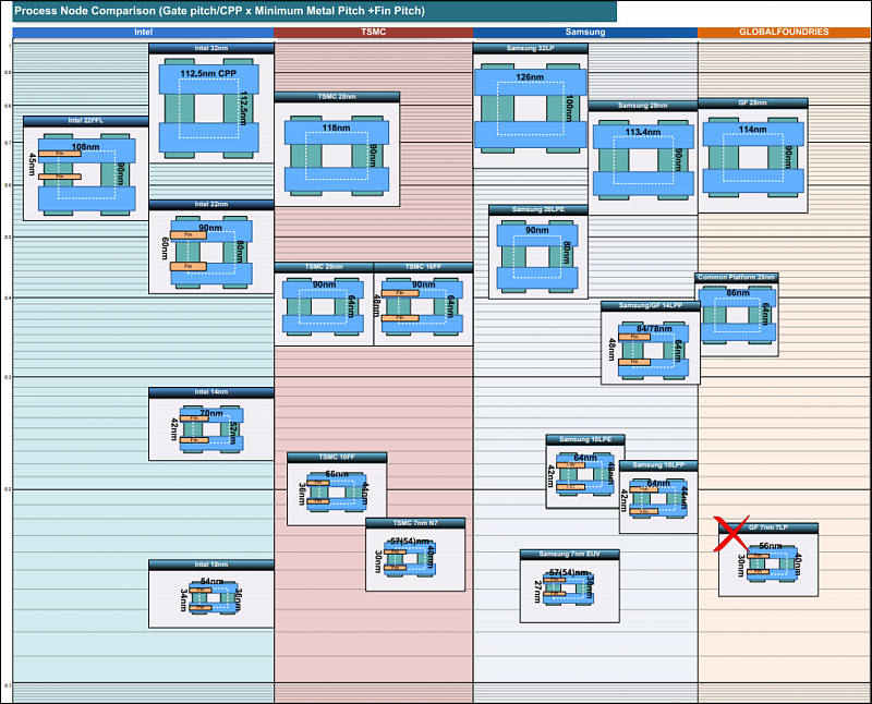
It is all fuzzy with Samsung, as their own chart above shows that they did not have any functioning 7nm line (that also poor Nvidia and other clients figured out hard).
 sa12304.jpg800 x 145 - 26K
 -
Nvidia expanses increased
And it is bad sign, as they need more and more people to do each new generation of GPUs.
 sa12292.jpg788 x 267 - 53K
 -
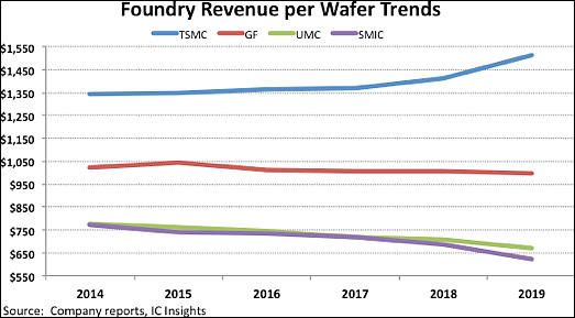
In 2019, TSMC was the only pure-play foundry manufacturing ICs using 7nm process technology. Not coincidentally, its overall revenue per wafer increased significantly as leading fabless IC suppliers lined up to have their newest designs manufactured on the 7nm process. TSMC was the only pure-play foundry that enjoyed higher revenue-per-wafer in 2019 (13%) compared to 2014. In contrast, 2019 revenue per wafer figures at GlobalFoundries, UMC, and SMIC—whose smallest process node is 12/14nm—were down by 2%, 14%, and 19% respectively, compared with 2014.

It is 2 players on the market already - TSMC and Samsung. Intel has around 20-25% last chance with their 7nm process, but they'll need to sell a lot of their empire for this.
 sa12286.jpg523 x 289 - 28K
 sa12285.jpg547 x 376 - 49K
 -
Intel is in talks to sell a unit that makes chips for home internet access gear to MaxLinear Inc.
No final decision has been made and Intel could keep the connected home division,
No, it won't. As Intel is short on money and they need money to stay among leading manufacturers and try to really make mythical 7nm.
We'll see big cuts in all departments this year also, as well as attempts to sell other parts.
-
Chinese smartphone maker, Oppo, is reportedly working on introducing its mobile application processors soon. A Chinese publication citing an official statement from an Oppo executive claims that component will be used in its in-house mobile APUs and could be called the Oppo M1 chipset.Oppo has also trademarked the processor at the European Union Intellectual Property Office (EUIPO) certification website. The company has hired some previous engineers of MediaTek and Spreadtrum to work on the chipset. Tony Chen, Oppo founder, and CEO has also highlighted that the company would spend around CNY 50 billion into R&D. One of the biggest impacts of Oppo introducing its processors will be a threat in the demand of Qualcomm-based chipsets as well as Samsung made Exynos SoCs.It will be interesting to see how Oppo will cut its reliance on Qualcomm. Given the company’s long-time partnership with the leading processor chip marker.
-
TSMC has started reducing its chip capacity support for Huawei, but is still working closely with the China-based vendor in the development for advanced 5nm and 3nm chip solutions.
And this is very dangerous. As can also mean the end of TSMC as leading suplier.
US very much wants Intel to be one, but they are failing.
-
Intel Corp. is laying off 128 workers at four locations at its Santa Clara headquarters.
The cuts follow the chipmaker's confirmation last month that it would cut roles as it shifts resources. The layoffs will take place by March 31, according to the filings with the EDD
And it is only small start.
-
Intel slashed Xeon prices, and by slashed we mean far more than 50%, but the MSRP didn’t change. Officially there was no change, that pipsqueak AMD has no effect on pricing, carry on folks and look away. Unofficially if you showed your friendly OEM a bid with an AMD CPU there were enough MeetComp dollars flowing to drop prices 2/3rds or more.
Xeon pricing will have huge impact on Intel.
Most probably we'll never see 7nm from them, especially if they will start having issues with notebook CPU prices (and this is second category with huge profits).
-
On CPU progress limits

CPU scaling has really slowed and there's just no two ways about it. It's not a marketing thing. It's a physics thing. And the ability for CPUs to continue to scale without increasing cost or increasing power has ended. And it's called the end of Dennard scaling. And so there has to be another approach.
 sa12241.jpg738 x 582 - 39K
 -
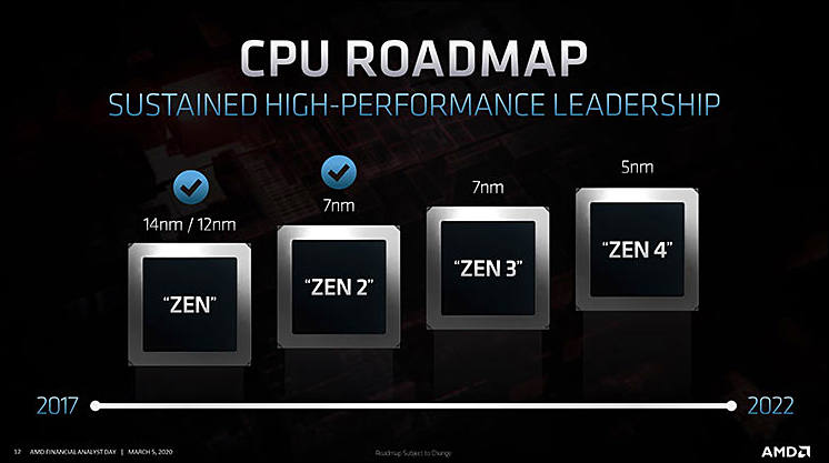
Good articles on 7nm AMD chips
AMD has reduced the size of the Core Complex (CCX), a cluster of Zen CPU cores, to about 50% of the 14-nm process generation by moving to the 7-nm process. Compared with the same amount of cache SRAM, the size is about half, and the density of transistors is almost doubled.
The size of CPU cores has also been reduced by half, and as a result, the number of CPU cores installed in the APU (Accelerated Processing Unit) aimed at the main stream has been doubled to eight.
However, this ratio is a bit strange, considering the miniaturization scenario of the conventional CMOS process.
AMD has skipped 10nm, the next process after 14nm, and is moving to a 7nm process. In the process node, the migration is for two generations. This means that the process has been reduced to 50% by miniaturizing the process for two generations. However, with traditional CMOS scaling, if the number of nodes is the same, the CPU core area should be 25%.
The traditional CMOS scaling rule states that a generation of process nodes reduces device area by 50%, thereby doubling transistor density. 4 times for 2 generations. In other words, the area should be 50% at 10nm from the 14nm process and 50% at 10nm to 7nm.
As a result, at 7 nm versus 14 nm, the same core die area is reduced to 25%. According to AMD, this is half the scale of traditional scaling.
-
Rumors are spreading that due to TSMC capacity issues and possible issues with 7nm EUV process, AMD can shift Ryzen 4000 release to November 2020 or even CES 2021.
-
Something interesting coming up or ASML shares
Intel got rid of all AMSL block of shares it owned (had been 15%), final parts had been sold during 2019.
Samsung and TSMC also sold all of their ASML stock.
It can't be good sign, as, most probably all companies see some HUGE problems ahead to act such.
-
L4 cache as dead end
“At some level, another level of cache is inevitable,” says Gianos. “We had a first level of cache and eventually we had a second. And eventually we added a third. And eventually we will have a fourth. It’s more of a question of when and why.
The architects at AMD, who did not want to be directly attributed because in having this conversation they did not want to be misconstrued with AMD promising that it would be adding L4 cache to the Epyc processor line – and to be clear, AMD has said nothing of the kind. But it did recognize that it is the next obvious thing to be thinking about, and just like Intel, believes that every architect is thinking about L4 caches, and it shared some of its thinking on background. Basically, AMD says that the tradeoff in number of cache layers and latency has been well studied in industry and academia, and that with each new cache layer, which is bigger, slower, and more widely accessed, there is a necessary tradeoff that increases the total path out to the DRAM because most designs would not continually speculatively access the cache layers further down in the hierarchy in parallel with cache tag lookup in the upper layers. This is exactly what Intel is also talking about above when Gianos says you need to find a balance between the hit rate and the capacity of the cache – and the L4 is no different.
Big L4 cache is expensive, eats silicon manufacturing capacity and do not bring much of performance increase outside of specific tasks.
-
Major issue - is money start flowing out of the bubble all things will stop


Howdy, Stranger!
It looks like you're new here. If you want to get involved, click one of these buttons!
Categories
- Topics List23,993
- Blog5,725
- General and News1,354
- Hacks and Patches1,153
- ↳ Top Settings33
- ↳ Beginners256
- ↳ Archives402
- ↳ Hacks News and Development56
- Cameras2,368
- ↳ Panasonic995
- ↳ Canon118
- ↳ Sony156
- ↳ Nikon96
- ↳ Pentax and Samsung70
- ↳ Olympus and Fujifilm102
- ↳ Compacts and Camcorders300
- ↳ Smartphones for video97
- ↳ Pro Video Cameras191
- ↳ BlackMagic and other raw cameras116
- Skill1,960
- ↳ Business and distribution66
- ↳ Preparation, scripts and legal38
- ↳ Art149
- ↳ Import, Convert, Exporting291
- ↳ Editors191
- ↳ Effects and stunts115
- ↳ Color grading197
- ↳ Sound and Music280
- ↳ Lighting96
- ↳ Software and storage tips266
- Gear5,420
- ↳ Filters, Adapters, Matte boxes344
- ↳ Lenses1,582
- ↳ Follow focus and gears93
- ↳ Sound499
- ↳ Lighting gear314
- ↳ Camera movement230
- ↳ Gimbals and copters302
- ↳ Rigs and related stuff273
- ↳ Power solutions83
- ↳ Monitors and viewfinders340
- ↳ Tripods and fluid heads139
- ↳ Storage286
- ↳ Computers and studio gear560
- ↳ VR and 3D248
- Showcase1,859
- Marketplace2,834
- Offtopic1,320


