It allows to keep PV going, with more focus towards AI, but keeping be one of the few truly independent places.
-
New AMD rumors
Present rumoprs are that APU Ryzen 6000 aka Rembrandt will use 6nm TSMC process.
It'll be slightly improved existing 7nm process with more EUV steps and little marketing adjustments.
Similar to fake 12nm AMD used before.
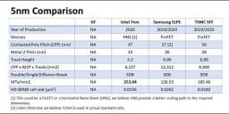
TSMC 5nm process is still very questionable and aimed at low power mobile chips.
3nm is just distant dreams for now.
Issue with 5nma dn 3nm considering CPU and GPU chips is that you no longer have enough surface to keep thermals good, as well as fact that with frequency rise transistor leaks become enormous.
-
Some new idiotism
"TSMC's enhanced 5nm process enters mass production in Q4, ahead of schedule.
AMD's new Ryzen first to adopt. PC competitive landscape may usher in the biggest change in 15 years."
-
TSMC capital expenditures will be reduced
Due to the impact of Huawei’s new ban, some customers’ orders of TSMC (2330) were revised down, which led to a conservative view of the annual revenue. Capital expenditure in 2020 will be 13% lower than the company's previous forecast and 9% less than the previous year.
After negotiations with semiconductor equipment vendors, it was found that some new equipment orders for TSMC have been extended from June to December. The latest plan shows that the 5-nanometer process is likely to be reduced by 10,000 to 15,000 pieces per month compared to the previous plan, and the 7-nanometer process may be reduced by 10,000 to 20,000 pieces. The combined capital expenditure in 2020 and 2021 will be reduced by 5 to 7 billion US dollars .
And it is big issue for TSMC, especially if later we'll see second wave.
-
And this is how the wall looks like
The American semiconductor industry is headed to Washington to push for $37 billion in federal funding to keep the industry competitive against China.
The SIA is asking for $5 billion in matched funding for a new semiconductor fab that would be operated in conjunction with a firm in the private sector — likely Intel. Intel CEO Bob Swan proposed in April that the company build a facility to work with the Pentagon on semiconductors for the defense sector. The SIA has earmarked a proposed $15 billion for states to provide incentives for the semiconductor industry to set up shop in their backyard, while the remaining $17 billion would be allocated for research and development funding.
As soon as smartphones sales no longer allow to move further firms look for the last option.
-
On why China still is pretty far from good position in this war
At the beginning of the semiconductor manufacturing process, monocrystalline silicon wafers are turned into chips. This procedure requires oxidation, coating, photolithography, etching, ion implantation, physical vapor deposition, chemical vapor deposition, polishing, wafer inspection and cleaning. Back-end processes include packaging and testing, backside thinning, wafer cutting, patching, wire bonding, molding, cutting tendon/forming, and final testing.
Semiconductor manufacturing equipment leading vendors
Oxidation/ RTP /laser annealing Applied Materials, Hitachi, Japan, Tokyo Electronics, Thermco, UK, Naura Technology Group Co., Beijing E-Town Semiconductor Technology
Glue development equipment
Tokyo Electronics, Deans, Germany SUSS, Austria EVG, Shenyang KingsemiLithography machines
ASML, Nikon Japan, Canon Japan, Tokyo Electronics, Applied Materials, Panlin Group, SEMES Korea, Shanghai Micro Electronics Equipment (Group) Co.Plasma etching machines
Pan Lin Group, Villian Semiconductor, Tokyo Electronics, Applied Materials, Hitachi, Japan JuSung, South Korea TES, AdvancedMicro-Fabrication Equipment Inc. China, North China ChuangIon implantation
Applied Materials, American Axcelies, German Ingun, American QA, American MicroXcat, Korean Leeno, Shanghai Kingstone Semiconductor, Beijing Zhongkexin Electronics Equipment, China Electronics Technology Group Corp.Physical vapor deposition
Applied Materials, Japan Evatec, Japan Ulvac, America Vaportech, Britain Teer, Switzerland Platit, Germany Cemecon, Beijing NMC Co., Sky Technology Development Co., Chengdu Rankuum Machinery, The 48th Research Institute of CETC, Cross-Tech Equipment Co.Chemical vapor deposition
Applied Materials, Panlin Group, American GT, Soitec, American ProtoFlex, French Semco, ASML, Tokyo Electronics, Nikon Japan, Canon Japan, North China Chuang, Shenyang Piotech Co.CMP equipment
Applied Materials, American Rtec, Japanese Evatec, HWatsing Technology, The 45th Research Institute of CETC, ACM ResearchWafer inspection: electrical inspection equipment, quality inspection equipment
Teradyne, Advantech, Tokyo Electronics, Corey Semiconductor, Applied Materials, Hitachi, Japan, Hangzhou Changchun Technology, Beijing Huafeng Test & Control Technology Co., Shanghai Zhongyi Automatic System Co., RISC Scientific Instrument (Shanghai) Co., Shanghai Jingce SemiconductorCleaning equipment
Japan Deans, Tokyo Electronics, Panlin Group, South Korea SEMES, North China Chuang, Shengmei Semiconductor, Pnc Process Systems Co., Shenzhen S.C. New Energy Technology Corp. -
TSMC is in talks with the US government about relevant subsidies for its new wafer fab in Arizona so that the foundry is able to implement the investment plan, said TSMC chairman Mark Liu at a press event right after the company's shareholders meeting on June 9.
Not only US taxpayer will pay for factory building. But they will also pay for each day of it working.
-
Present data is that TSMC wants up to $25 billions USD from US goverment. This is size of special US fund for semiconductor productiona nd development. It is expected that TSMC and Intel will get up to 95% of this fund.
Without such taxpayer money semiconductor inductry can no longer develop, and it is only ont he approach to the hard wall.
-
Another Intel top manager bites the dust
Intel announced that Jim Keller has resigned effective June 11, 2020, due to personal reasons. Intel appreciates Mr. Keller's work over the past two years helping them continue advancing Intel's product leadership and they wish him and his family all the best for the future. Intel is pleased to announce, however, that Mr. Keller has agreed to serve as a consultant for six months to assist with the transition.
Intel has a vastly experienced team of technical leaders within its Technology, Systems Architecture and Client Group (TSCG) under the leadership of Dr. Venkata (Murthy) Renduchintala, group president of TSCG and chief engineering officer. As part of this transition, the following leadership changes will be made, effective immediately:
-
Supply chain partners of AMD, Nvidia and Intel have been left confused recently by the chip vendors' product launch schedules, which have either been changed frequently or kept a secret in their latest rounds of competition.
Issue with schedules is more related to TSMC and overall economcs situation.
It is now clear that something is up with so called TSMC 5nm process and that TSMC had been unablle to make 7nm+ process that uses EUV to work reliably still.
-
TSMC will enter production using 5nm process technology later in June for Apple's custom-designed A14 processor and Qualcomm's Snapdragon X60 modem,
Rumors are that we can expect as much as 30% price hike for products made with 5nm TSMC process and around 20% for 7nm+ process (if they made it work finally).
Numeber of defective chips now is very high, hence TSMC even asked US to put sanctions on Huawei, as otherwise issues could become too public.
-
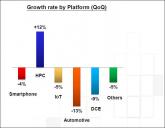
Glogal ODM smartphone shipments are expected to reach 260 million units in 2020, down 41.6 million units or 13.5% from a year earlier, according to Digitimes Research.
Hard times coming for chipmakers.
-
TSMC R&D spending hit an all-time high of nearly US$3 billion last year.
TSMC disclosed in its annual report that R&D expenses grew about 4% on year to US$2.959 billion in 2019. The R&D spending accounted for 8.5% of the dedicated IC foundry's overall revenues last year, which came to a record high of NT$1.07 trillion.
TSMC also scaled up its R&D workforce to 6,534 employees in 2019, up 5% on year, according to the Taiwan-based foundry.
Sudden issues of TSMC can now mean full stop of all industry with unknown consequences.
-
Samsung Electronics has revised its foundry process roadmap, skipping 4nm and jumping directly to 3nm from 5nm, according to industry sources.
Big issues at Samsung.
Also note that despite loud claims Samsung still do not make any significant amoung of complex chips using their 8nm process. Rumors are that both Apple and Nvidia tried to use it but failed.
-
In 2019, demand from semiconductor companies in Taiwan including TSMC, UMC, VIS, Powerchip, Macronix, Winbond, Micron, ASE/SPIL and Powertech for materials reached an amount of NT$330.6 billion (US$11.22 billion), accounting for 22% of the worldwide value while that for equipment was NT$513 billion, or a global share of 28%.
Semiconductor companies plan to expand their capacities, their investments in the next couple of years will reach as high as NT$2.72 trillion.
Taiwan is very worried, as its position is very bad in the conflict between US and China, as both of countries can wreck all the taiwan economy to ashes in few months.
Also leakage of top qualified engineers is staggering, for example Huawei now hires any silicon related engineers for 4-5x of their present taiwan salary.
-
The board of directors of Taiwan Semiconductor Manufacturing Company (TSMC) has approved plans to issue NT$13.9 billion (US$471.7 million) in unsecured bonds to help purchase new equipment and facilities for capacity expansion, according to the world's largest dedicated semiconductor foundry.
TSMC already sold NT$60 billion in unsecured bonds in the first half of 2020. Proceeds from the bond sale are for the foundry's 5nm process capacity expansion at its new Fab 18 in the Southern Taiwan Science Park (STSP).
As firms no longer sell enough top smartphones TSMC need to ask for money, including tens of billions of free US money they wil get for banning Huawei (and China will never forget this, expect few extreme strikes aimed precisely at TSMC in next few months).
-
Chinese give more money to companies related to chips production
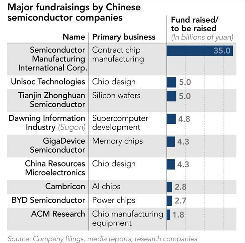
 sa13680.jpg800 x 794 - 100K
 -
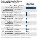
Why TSMC so wanted to drop Huawei
Actually N7FF+ has big issues and new Huawei chip is the only one using it.
 sa13757.jpg637 x 349 - 38K
 -
On EUV
To accelerate the development of EUV lithography technology, ASML invited Intel, Samsung and TSMC to become its shareholders in 2012, raising sufficient funds to support its development of ever-more advanced EUV lithography equipment compatible with both 12-inch and 18-inch wafers.
ASML is now the world's only supplier of EUV scanners, which entail up to US$100 million in unit production cost, and Gudeng is the only Taiwanese maker as well as one of the world's only two ASML-validated suppliers of EUV reticle inner pods for such scanners, with each pod needed to protect, transmit and store each EUV reticle mask.
We have absolute monopoly now that is directly controlled by US and partly by EU.
-
China’s biggest chipmaker SMIC is set to follow its staggering $6.6 billion share sale with its Shanghai market debut on Thursday.
It is big money shortages and we can observe how all leading manufacturers started to get financing directly from states.
-
Battle for ASML secrets and people will be epyc
Major thing that China needs to destroy any US competition is access to knowledge of ASML and their close suppliers.
It will be huge battle of special forces, lot of special agreements with people travelling on private jets, secret kidnappings, cyber attacks and much more.
-
TSMC expects to see 5nm process technology account for about 8% of its total wafer revenue in 2020, compared with the about 10% estimated previously. The foundry also confirmed it has stopped taking new orders from Huawei.
If not ban on Huawei to stop 7nm EUV non working process as well as allow around double faulty 5nm dies (as process is still bad even with Apple moving production much further!) - it could be big scandal.
-
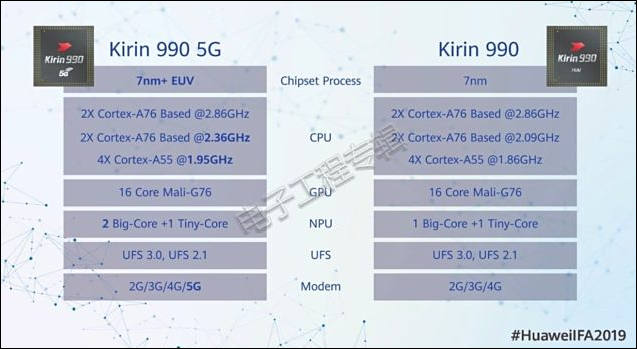
And changes are fully opposite to TSMC management predictions
 sa13779.jpg669 x 519 - 37K
 -
TSMC just needs money
The Japanese government is considering having Taiwan Semiconductor Manufacturing Co. ally with a local maker or research institution.
The government could offer funding support totaling several 100 billion yen provided the overseas maker initated a joint development project with local partnerships, the report said, potentially having factories built in Japan.
As smartphone buyes do not longer want ot buy overpriced junk TSMC now need direct interference of leading capitalist states.
Expect TSMC to become one of the main battelefields between US and China, as former now prepares retaliation strike that can even stop all chips production. Stay tuned.


Howdy, Stranger!
It looks like you're new here. If you want to get involved, click one of these buttons!
Categories
- Topics List23,991
- Blog5,725
- General and News1,354
- Hacks and Patches1,153
- ↳ Top Settings33
- ↳ Beginners256
- ↳ Archives402
- ↳ Hacks News and Development56
- Cameras2,367
- ↳ Panasonic995
- ↳ Canon118
- ↳ Sony156
- ↳ Nikon96
- ↳ Pentax and Samsung70
- ↳ Olympus and Fujifilm101
- ↳ Compacts and Camcorders300
- ↳ Smartphones for video97
- ↳ Pro Video Cameras191
- ↳ BlackMagic and other raw cameras116
- Skill1,960
- ↳ Business and distribution66
- ↳ Preparation, scripts and legal38
- ↳ Art149
- ↳ Import, Convert, Exporting291
- ↳ Editors191
- ↳ Effects and stunts115
- ↳ Color grading197
- ↳ Sound and Music280
- ↳ Lighting96
- ↳ Software and storage tips266
- Gear5,420
- ↳ Filters, Adapters, Matte boxes344
- ↳ Lenses1,582
- ↳ Follow focus and gears93
- ↳ Sound499
- ↳ Lighting gear314
- ↳ Camera movement230
- ↳ Gimbals and copters302
- ↳ Rigs and related stuff273
- ↳ Power solutions83
- ↳ Monitors and viewfinders340
- ↳ Tripods and fluid heads139
- ↳ Storage286
- ↳ Computers and studio gear560
- ↳ VR and 3D248
- Showcase1,859
- Marketplace2,834
- Offtopic1,319


