-
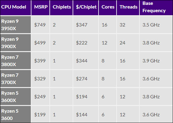
On why CPUs are so heavily guarded
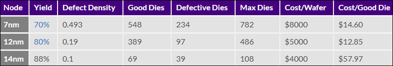
Note that 1st gen Ryzen costs make no sense here.
And here is per chiplet money that AMD gets:
 sa9269.jpg799 x 135 - 28K
 sa9270.jpg567 x 404 - 38K
 -
Ryzen 3xxx supply is really bad now
AMD is saved by preorders and promises, but real supply is quite low and can't keep up with orders.
AMD already postponed announcement 2 times, but due to quite low TSMC yields and due to fact that 7nm lines are fully loaded with Apple and Huawei chips, they can't do better.
Rumors are that up to 30% of AMD chips go to trash bin being fully functional as they can't keep the frequency standards, many works properly only up to 2-2.3Ghz.
-
Dreams about 3D stacking from company who lost the battle already
GLOBALFOUNDRIES, the world’s leading specialty foundry, today announced that it has taped-out an Arm®-based 3D high-density test chip that will enable a new level of system performance and power efficiency for computing applications such as AI/ML and high-end consumer mobile and wireless solutions. The new chip was fabricated using GF’s 12nm Leading-Performance (12LP) FinFET process and features Arm’s mesh interconnect technology in 3D that allows data to take a more direct path to other cores, minimizing latency while increasing data transfer rates as demanded by data centers, edge computing and high-end consumer applications.
The delivery of this chip demonstrates the fast progress that Arm and GF are making in researching and developing differentiated solutions that enable improvements in device density and performance for scalable high-performance computing. Moreover, the companies validated a 3D Design-for-Test (DFT) methodology, using GF’s hybrid wafer-to-wafer bonding that can enable up to 1 million 3D connections per mm2, extending the ability to scale 12nm designs long into the future.
“Arm’s interconnect technology in 3D enables the semiconductor industry to augment Moore’s Law to address a greater diversity of computing applications,” said Eric Hennenhoefer, vice president, Arm Research. “GF’s expertise in fabrication and advanced packaging capabilities, combined with Arm technology, gives our mutual partners additional differentiation to venture into new paradigms for next generation, high-performance computing.”
-
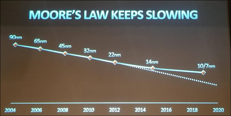
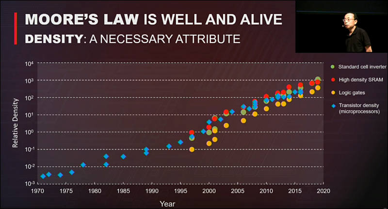
TSMC on Moore Law
First, let's discuss the elephant in the room. Some people believe that Moore's Law is dead because they believe it is no longer possible to continue to shrink the transistor any further. Just to give you an idea of the scale of the modern transistor, the typical gate is about 20 nanometers long. A water molecule is only 2.75 Angstrom or 0.275 nanometer in diameter! You can now start counting the number of atoms in a transistor. At this scale, many factors limit the fabrication of the transistor. The primary challenge is the control of materials at the atomic level. How do you place individual atoms to create a transistor? How do you do this for billions of transistors found on a modern chip? How do you build these chips that have billions of transistors in a cost effective manner?
To address this squarely, TSMC has recently announced our N5P node which further expands our leadership beyond the N5 node that will feature the world’s highest transistor density and offer the fastest performance. After being exposed to our technology roadmap, I can safely state that TSMC has many years of pioneering and innovation ahead of us where we will continue to shrink the individual transistor and continue to improve density. You will hear more from us in the coming months and years as we progress to new nodes.
Beyond the individual transistor, we also need to look at the system level density. Circling back and looking at the classic compute tasks of CPUs and GPUs, the modern chip has extremely fast transistor clock speeds that approach 5 gigahertz and beyond. The central challenge to these compute tasks is actually to keep the CPU and GPU cores fed with data. While this is classically a software challenge, modern architectures and methods for threading have squarely put the performance bottleneck at the hardware level. We have finally seen the limitations of memory caching in the era of big data analytics and AI.
To feed modern fast CPUs, GPUs and dedicated AI Processors, it is critical to provide memory that is both physically closer to the cores that are requesting the data for improved latency, in addition to supplying a higher bandwidth of data for the cores to process. This is what device level density provides. When memory is collocated closer to the logic cores, the system achieves lower latency, lower power consumption and higher overall performance.
Some of you may think that this is a system level concern and not an intrinsic attribute of a device technology. This may be strictly true in the past but the line is already getting blurry between the definition of a chip and the definition of a system. The line will continue to get more blurry and eventually will be completely eliminated. We have now transitioned from an era of design-technology co-optimization (DTCO) to system-technology co-optimization (STCO).
https://www.tsmc.com/english/newsEvents/blog_article_20190814.htm
-
Ryzen 7nm chips can have serious issues with reliability
The original limits for Ryzen 3000 SKUs were:
- 3600 = 4100MHz (80-95°C) / 4200MHz (< 80°C)
- 3600X = 4200MHz (80-95°C) / 4400MHz (< 80°C)
- 3700X = 4200MHz (80-95°C) / 4400MHz (< 80°C)
- 3800X = 4300MHz (80-95°C) / 4550MHz (< 80°C)
- 3900X = 4400MHz (80-95°C) / 4650MHz (< 80°C)
Since then, it appears that the HighTemperature limit has been reduced further to 75°C (from 80°C). New SMUs also have introduced "MiddleTemperature" limit, but that gets disabled when PBO is enabled.
AMD privately discovered fast degradation of CPU dies due to small 7nm process, such fats that it can break within warranty period.
Reliability of Sandy Bridge 32nm CPUs is around 10x-15x more compared to current 7nm process, and it still runs on same or higher clocks. Issue with new process is extreme leaks that can be up to 10x larger than on old processes.
-
The lead time for production of 7nm chips at Taiwan Semiconductor Manufacturing Company (TSMC) has extended to nearly six months from the previous two months because of strong demand, according to industry sources.
It is not much of demand issue, but issue of still quite low yields. Hence AMD design optimized for large number of defects.
-
Intel still has high hopes
GlobalFoundries laying off more than 400 workers at its Fab 8 computer chip factory in Malta last year may have benefited Intel. The staff were laid off after GloFlo decided not to bother with 7nm and to stick with the current cutting-edge 14-nanometre chips, GlobalFoundries was able to reduce its research and development expenses significantly.
Intel is building a $7 billion chip factory known as Fab 42 outside of Chandler, Arizona that is expected to make 7-nanometre chips eventually, and former GlobalFoundries workers that had been part of the 7-nanometre team at Fab 8 would be valuable to Intel as it gets its Fab 42 up and running.
According to LinkedIn dozens of former GlobalFoundries employees have found a home with Intel.
Best Intel hopes now are that to invest funds will want to keep two modern process manufacturers, despite any costs. Otherwise we can see slow Intel demise as 10nm process is clearly total failure for now.
-
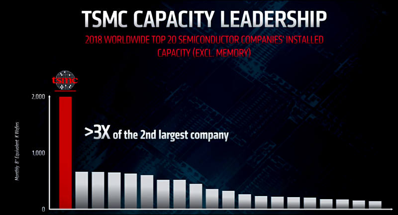
TSMC
TSMC has advised its clients to book foundry capacity well in advance for their 7nm chip demand for the entire 2020, according to industry sources.
7nm issues continue. Now TSMC owners artificially hold 7nm production as they are happy with profits and have no idea how to fix low yields.
TSMC is expected to see its revenues in the second half of 2019 jump 32% from the first half - more than three times the 10% growth rate expected for the entire IC industry during the same period, IC Insights said. "There is little doubt that 7nm application processors for new smartphones from Apple and Huawei are driving the forecast for a strong second-half rebound in TSMC's sales".
Yes, TSMC and Apple with AMD are ripping you big part with 7nm.
TSMCis expected to have over 7x the dollar volume sales at sub-40nm processes as compared to the combined 2019 total of Globalfoundries, UMC, and SMIC (US$22.9 billion versus US$3.2 billion)
Here we have actual monopoly.
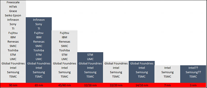
It took eight quarters for the foundry's 40-45nm technology to secure greater than 20% of its total sales, five quarters for its 28nm process to exceed that threshold, and only three quarters for its 7nm process to account for more than 20% of its quarterly revenue.
And it is growing fast.
-
Rumor came out today that Intel had canceled all plans for 10nm desktop processors, leaving a void until the company would introduce 7nm desktop processors in 2022.
Intel response:
"We continue to make great progress on 10nm, and our current roadmap of 10nm products includes desktop."
Roadmap only now and desktop can mean also Xeon type HEDT chips.
It is all very fishy, as most probably 10nm is the totally dead process, but one that have tens of billions USD invested, so sad to drop it totally.
Intel claims that 7nm will be simpler is total and utter bullshit.
-
TSMC and EUV
On Oct. 7, the world’s largest foundry announced that its 7nm plus (N7+) node has become the industry’s first commercially available (extreme ultra-violet) EUV technology. TSMC said in a press statement that it has been quickly deploying capacity to meet N7+ demand driven by multiple customers
The leading edge is currently at 7+ with about three layers done using EUV, he says. In 2020, TSMC will ramp 5nm in the second half with significantly increased EUV usage of about 15 layers, followed by 6nm ramping at the end of 2020 with about four layers done in EUV
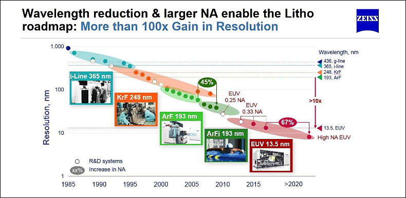
Huawei will lead at 5nm followed by Apple, both seeking to take advantage of die-size benefits plus normal power and speed improvements, he says. In the meantime, MediaTek is likely to be TSMC’s leading customer at the 6nm node due to persistent limited wafer availability on 7nm.
EUV provides a roughly 20 percent reduction in mask levels, which in turn cuts production cycle time, according to Samsung. Chip designers who take advantage of EUV processes can avoid the triple- and quadruple-patterning techniques that fabs have struggled with while using 193nm immersion lithography.
Samsung introduced EUV with their 7LPP node late last year, with production used internally for Samsung’s application processors and possibly Qualcomm, but not in high volume. Samsung has plans for 6nm EUV next year and 5nm EUV in development with likely volume in 2021.
TSMC, Samsung and Intel — are planning to adopt EUV in their production roadmaps.
Originally, Intel’s 7nm generation was slated for introduction in 2017, but delays in 14nm and 10nm delayed the company's planned launch of 7nm MPUs to 2021. In May 2019, Intel executives claimed the company's 7nm technology would challenge the performance of 5nm processes planned by TSMC
Things are really bad now.
We have TSMC as leader that can only do 3 layers and very limited batches and almost all volume will go to AMD during next year. I think we must expect multiple issues as we had this year, hidden behind closed doors for a while. Most probably AMD will be forced to move 7+ consumer processors introduction to late 2020 or even 2021. Focusing on EPYC chips with huge margins for now.
Samsung is also very bleak. They can do lot of nice NAND and DRAM, but at processors they like to lie. Next year we can see various fake declarations.
Intel just do not know that to do. Their only hope is completely non ready 7nm process, and they want to repeat all 10nm errors. Now it is loud declarations about 2021 that will become 2022 and most probably 2023-2024 for first consumer chips.
Intel will be definitely supported at all costs via special bank loans and direct injections and similar things. As it is very risky to have only leader located in Taiwan, as you can totally lost access to it within few days if China will decide to invade Taiwan 9and this is quite probable within next 5 years).
 sa10504.jpg790 x 386 - 60K
 -
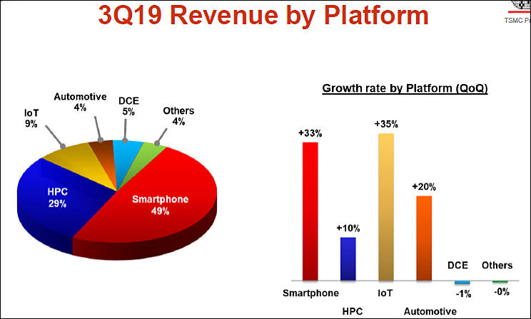
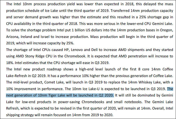
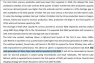
From TSMC report

 sa10505.jpg747 x 449 - 58K
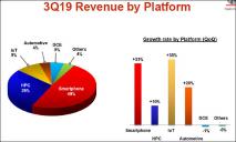 sa10506.jpg744 x 448 - 44K
 -
Fast improvements (due to cores number) seems to be up.
AMD now want to move into marketing strategy and tick-tock approach. With each second model being extremely small improvements. Yes, 3-5% a year with 10-25% price rise each time.
-
“While Intel will theoretically have 7nm parts out sometime in 2021...we believe it likely that CPU and other mainstream 7nm parts will not be on the road map until late that year, if not sometime in 2022.”
By the time Intel gets 7nm production going, TSMC will likely be making 3nm chips for much of Intel’s 7nm lifespan.
“Hence any hopes of Intel’s ability to ‘close the process gap’ seem forlorn, unless TSMC drops the ball (which, as of this moment, they are showing no signs of)”
-
Huawei's HiSilicon has unseated Apple as the largest customer of TSMC in terms of advanced process node capacity share, according to industry sources.
Competition of doomed runners :-)
-
Moore’s law, which is widely known, is the observation that the number of transistors in a leading-edge integrated circuit doubles about every two years.
Moore’s Second Law, which is less well known, states that the capital cost of a leading-edge semiconductor fab increases exponentially over time.
Semiconductor industry history shows us that once a company falls out of the leading-edge process race and moves to foundry model, it does not get back into the fab business. The foundry model plays to Moore’s Second Law by aggregating fab needs of these fabless players.
Critical time passed with half measures and Intel has now come to a stage where building on the current internal foundry model is increasingly infeasible and the x86 riches may no longer support a place at the front of the leading edge.
The revised capex budget TSMC presented at its recent Q3 earnings call - $14B to $15B for 2019 and likely a similar amount for 2020. TSMC, has reached approximate capex parity with Intel in spite of roughly half the revenues.
Intel will now have to increase its capex as a percentage of revenues. The problem is that Intel’s revenue opportunity is shrinking due to market share gains from AMD. On the other hand, TSMC revenues are growing leaving TSMC with the ability to spend more capex if it so desires. Intel’s margins will be reducing due to assault from AMD and increased capex spread over lower volumes.
Intel should be two distinct businesses:
- A cutting-edge semiconductor design company focusing primarily on CPUs and GPUs. This part of the company, despite recent under performance against AMD, is a potent organization. Chances of this group gaining back performance leadership are high.
- A fab that has underperformed recently, is facing dis-economies of scale governed by Moore’s Second Law and is likely to fall further and further behind.
Samsung, having fallen behind TSMC at 7nm, is in a similar situation. If there is strategic desire, and we believe that there is plenty, there is an opportunity for these players to consolidate their forces and create a viable foundry alternative to TSMC.
Intel has lost its process leadership to TSMC and the company is unlikely to get back to its top dog position in the industry.
While possibilities such as divesting fab operations and integrating them with Samsung fab operations exist and may be implemented, the organizational inertia at Intel makes the timing of such moves questionable. Given this reality, we find it highly likely that Intel has now forever lost its process leadership and will suffer immensely as a result.
 sa10585.jpg800 x 342 - 42K
 -
TSMC is expected to step up the construction of its advanced 3nm wafer fab after securing 30 hectares of land in the Southern Taiwan Science Park (STSP) by the end of 2019, according to industry sources.
PR is everything :-)
-
China's National Integrated Circuit Industry Investment Fund (Big Fund) on October 22 set up a new fund of CNY204.15 billion (US$28.9 billion), marking the start of its second-phase support for domestic chipmakers, according to China company registration information.
Fund already spent an estimated CNY138.7 billion on its first-phase capital support for the local chip industry.
China is late to the party, and also does not have expertise in making equipment (that had been intentionally monopolized previously to control knowledge spread).
Real required investments now exceed $250-300 billions to just match 10-12nm process with enough volume required, and another $50-100 to match existing 7nm TSMC (without EUV).
-
AMD still do not want to make public bad situation with 7nm yields and total processors availability.
TSMC now can't provide enough good 7nm plates. main priority goes to leading mobile LSIs as most profitable, later goes AMD chipsets for EPYC. All else is produced only if they have capacity.


Howdy, Stranger!
It looks like you're new here. If you want to get involved, click one of these buttons!
Categories
- Topics List23,991
- Blog5,725
- General and News1,354
- Hacks and Patches1,153
- ↳ Top Settings33
- ↳ Beginners256
- ↳ Archives402
- ↳ Hacks News and Development56
- Cameras2,367
- ↳ Panasonic995
- ↳ Canon118
- ↳ Sony156
- ↳ Nikon96
- ↳ Pentax and Samsung70
- ↳ Olympus and Fujifilm101
- ↳ Compacts and Camcorders300
- ↳ Smartphones for video97
- ↳ Pro Video Cameras191
- ↳ BlackMagic and other raw cameras116
- Skill1,960
- ↳ Business and distribution66
- ↳ Preparation, scripts and legal38
- ↳ Art149
- ↳ Import, Convert, Exporting291
- ↳ Editors191
- ↳ Effects and stunts115
- ↳ Color grading197
- ↳ Sound and Music280
- ↳ Lighting96
- ↳ Software and storage tips266
- Gear5,420
- ↳ Filters, Adapters, Matte boxes344
- ↳ Lenses1,582
- ↳ Follow focus and gears93
- ↳ Sound499
- ↳ Lighting gear314
- ↳ Camera movement230
- ↳ Gimbals and copters302
- ↳ Rigs and related stuff273
- ↳ Power solutions83
- ↳ Monitors and viewfinders340
- ↳ Tripods and fluid heads139
- ↳ Storage286
- ↳ Computers and studio gear560
- ↳ VR and 3D248
- Showcase1,859
- Marketplace2,834
- Offtopic1,319


