-
According to our sources, ATIC (Which owns about nine-tens of Globalfoundries) is in the process of looking for potential buyers for GlobalFoundries.
Nice.
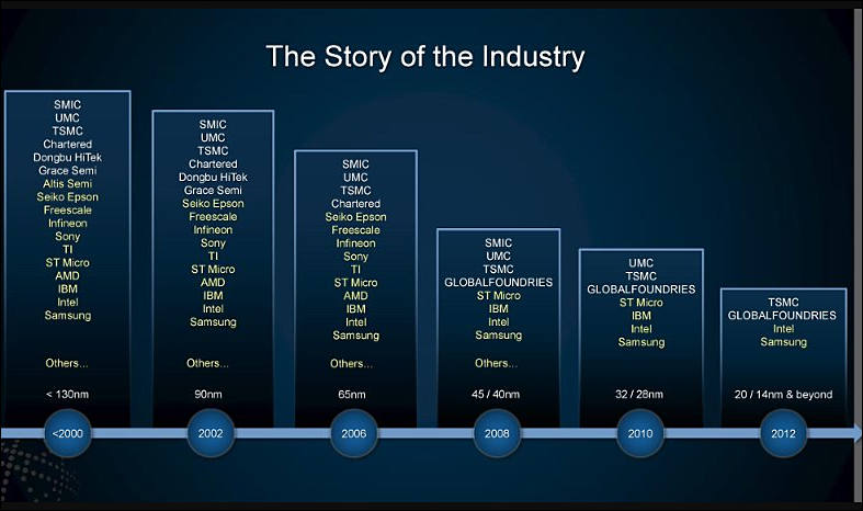
So from 4 remaining competitors:
- GlobalFoundries cancelled new technology, out of competition and will do 14nm and less only
- Intel has huge issues with 10nm (it is actually same or even better than others 7nm)
- TSMC use huge Apple money and seems to be on track for 7nm (yet not fully true 7nm)
- Samsung is similar to TSMC, but can also use their own big smartphones profits
-
In perspective
Ten little Soldier Boys went out to dine;
One choked his little self and then there were nine.Nine little Soldier Boys sat up very late;
One overslept himself and then there were eight.Eight little Soldier Boys travelling in Devon;
One said he'd stay there and then there were seven.Seven little Soldier Boys chopping up sticks;
One chopped himself in halves and then there were six.Six little Soldier Boys playing with a hive;
A bumblebee stung one and then there were five.Five little Soldier Boys going in for law;
One got in Chancery and then there were four.Four little Soldier Boys going out to sea;
A red herring swallowed one and then there were three.Three little Soldier Boys walking in the zoo;
A big bear hugged one and then there were two.Two little Soldier Boys sitting in the sun;
One got frizzled up and then there was one .One little Soldier Boy left all alone;
He went out and hanged himself and then there were none. sa4464.jpg787 x 466 - 52K
 -
At 7mm we lost another player - GLOBALFOUNDRIES
GF is realigning its leading-edge FinFET roadmap to serve the next wave of clients that will adopt the technology in the coming years. The company will shift development resources to make its 14/12nm FinFET platform more relevant to these clients, delivering a range of innovative IP and features including RF, embedded memory, low power and more. To support this transition, GF is putting its 7nm FinFET program on hold indefinitely and restructuring its research and development teams to support its enhanced portfolio initiatives. This will require a workforce reduction, however a significant number of top technologists will be redeployed on 14/12nm FinFET derivatives and other differentiated offerings.
-
Stop already happened for Intel and it'll go back
What Intel is not telling you, or the analysts, is that the 10nm you may get in late 2019 is not the 10nm they had intended to come out in 2015. More importantly this new process is a significant step backward from the 10nm they promised, as touted in their manufacturing day. How much of a step backwards? Several of SemiAccurate’s moles are saying it is effectively a 12nm process rather than a 10nm process, and the technical changes more than back that claim up.
https://semiaccurate.com/2018/08/02/intel-guts-10nm-to-get-it-out-the-door/
-
Intel expect no progress with 10nm until second half of 2019, at best
 sa3937.jpg735 x 428 - 107K
 -
10nm Ice Lake based Xeon chips are postponed, They won't appear in 2019 and could be moved as far as 2021-22.
-
Problems now affect notebook vendors
Global notebook vendors including HP, Dell, Lenovo, Acer and Asustek Computer will be unable to launch new models fitted with Intel's new-generation CPUs in the second half of 2018 as scheduled, as the release of Intel's new offerings will not come soon enough for this year's high season
-
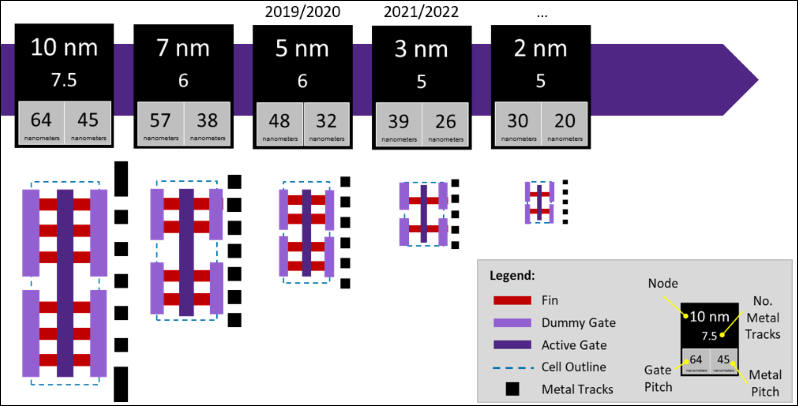
New tech to pack more stuff
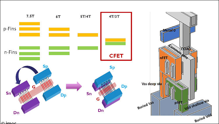
At this week’s 2018 Symposia on VLSI Technology and Circuits, imec, the world-leading research and innovation hub in nanoelectronics and digital technology, will present a process flow for a complementary FET (CFET) device for nodes beyond N3. The proposed CFET can eventually outperform FinFETs and meet the N3 requirements for power and performance. It offers a potential area scaling of both standard cells (SDC) and memory SRAM cells by 50%.
-
7nm progress
Taiwan Semiconductor Manufacturing Company (TSMC) has started commercial production of chips built using 7nm process technology.
TSMC will tape out more than 50 chip designs with its 7nm process technology by the end of 2018, Wei said. AI, GPU and cryptocurrency applications take up the majority of the tape-outs, followed by 5G and application processors.
TSMC will also start taping out chips built using an enhanced 7nm node with EUV in the second half of 2018.
5nm plans
TSMC's 5nm node's risk production is scheduled to kick off in the first half of 2019, with mass production at the end of the year or the beginning of 2020,
-
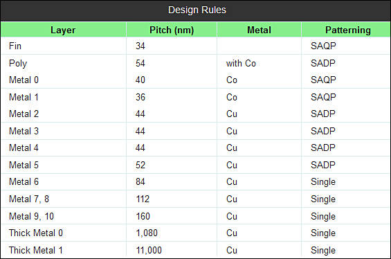
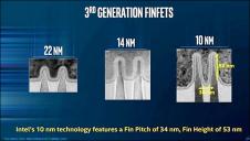
Details on Intel 10nm

- Logic transistor density of 100.8 mega transistors per mm2, increasing 10nm density 2.7X over the 14nm node
- Utilizes third generation FinFET technology
- Minimum gate pitch of Intel’s 10 nm process shrinks from 70 nm to 54 nm
- Minimum metal pitch shrinks from 52 nm to 36 nm
Process Highlights:
- Deepest scaled pitches of current 10 nm and upcoming 7 nm technologies
- First Co metallization and Ru usage in BEOL
- New self-aligned patterning schemes at contact and BEOL
SRAM improvements
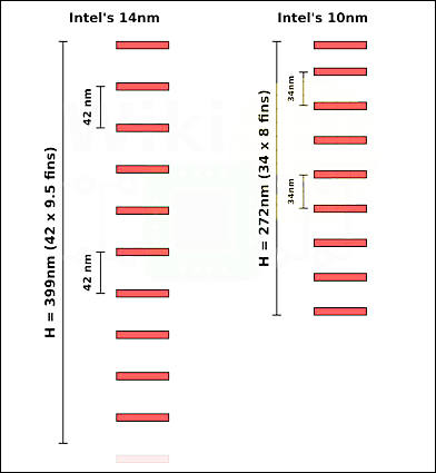
Moving contact to reduce footprint
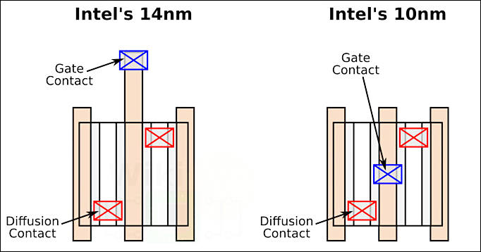
Metallization layers
 sa3616.jpg625 x 354 - 38K
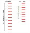 sa3617.jpg392 x 425 - 21K
 sa3618.jpg682 x 358 - 39K
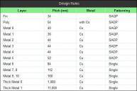 sa3619.jpg565 x 374 - 44K
 -
TSMC moved its 7nm process dubbed N7 to volume production in the second quarter of 2018. The foundry expects sales generated from the node to account for over 20% in the fourth quarter of 2018 and 10% in all of the year. In addition to mobile devices, server CPU, network processors, gaming, GPU, FPGA, cryptocurrency, automotive and AI are the target applications of the N7.
An improved version of TSMC's N7 technology, dubbed N7 Plus, will adopt EUV lithography technology and become available in 2019, according to the foundry.
Wall hit will be very hard for industry it seems.
-
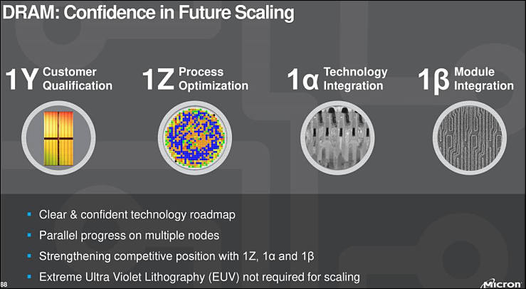
Micro thinks that EUV not required for DRAM scaling, for now at least
 sa3511.jpg739 x 406 - 47K
 -
Samsung Process Technology Roadmap Updates
- 7LPP (7nm Low Power Plus): 7LPP, the first semiconductor process technology to use an EUV lithography solution, is scheduled to be ready for production in the second half of this year. Key IPs are under development, aiming to be completed by the first half of 2019.
- 5LPE (5nm Low Power Early): Through further smart innovation from the 7LPP process, 5LPE will allow greater area scaling and ultra-low power benefits.
- 4LPE/LPP (4nm Low Power Early/Plus): The use of highly mature and verified FinFET technology will be extended to the 4nm process. As the last generation of FinFET, 4nm provides a smaller cell size, improved performance, and faster ramp-up to the stable level of yield by adopting proven 5LPE, supporting easy migration.
- 3GAAE/GAAP (3nm Gate-All-Around Early/Plus): 3nm process nodes adopt GAA, the next-generation device architecture. To overcome the physical scaling and performance limitations of the FinFET architecture, Samsung is developing its unique GAA technology, MBCFET (Multi-Bridge-Channel FET) that uses a nano-sheet device. By enhancing the gate control, the performance of 3nm nodes will be significantly improved.
-
Let's talk about the Company's sort of core leadership in manufacturing technology. I mean obviously Intel was the foundational architect of Moore's Law. The team has had a solid track record of driving performance, combination of you know your leadership in driving Moore's law and silicon process technology as well as architectural innovations as well. And you know just a little bit over a year ago at your Investor Day, the team described Intel being on track to scale logic scale area at a rate of 0.5x every two years, this is from a process technology perspective. Moreover at that event, you discuss Intel having an approximately three-year lead when versus competitors launching equivalent 10 nanometer processes.
Fast forward to today, Intel has delayed the high volume ramp of 10 nanometer, and with the leading foundry guys in the market bringing 7 nanometer products to the market maybe second half of this year arguably with similar sales and area type of benefits, as 10 nanometers, the markets getting a bit concerned that the gap is closing, and this potentially leads to the gap also closing between you and some of your competitors that take advantage of those process technology. So first off, could you just help us understand why Intel has made the decision to delay the 10 nanometer technology?
Murthy Renduchintala
Sure. Well and first of all, I think that silicon leadership is really important in as much as it supports product leadership. Silicon leadership in and of itself is only one of the aspects required. First of all Intel is a product company, it's not necessarily focused on being a merchant foundry. And in addition to silicon leadership, you really also need right architectural capability, the ability to execute silicon programs to predictable timelines, and you need an arsenal of capabilities and packaging, assembly and test technologies. So bringing all of those the weather is really what drives product leadership.
In terms of 10-nanometer, we are shipping 10-nanometer in low volumes. I think that if you go back to when we originally defined the recipe of 10-nanometer back in early 2014, we defined some very aggressive goals for our second-generation hyper-scaling. We targeted a 2.7x scaling factor, from 14-nanometers which was in the very stages of product ramp at that point in time. And 14-nanometers with in and of itself of 2.4x scaling on 22 nanometers, so clearly our engineering team in TMG had very, very ambitious goals in terms of the transistor scaling required.
That required a lot of innovations to come together and maybe those plans were a little bit more aggressive in hindsight than was ideal. And so, therefore we had a little bit of a greater challenge in bringing 10-nanometer to market than we had originally expected. However, the issues that we faced in getting that to prime time yield and not fundamental. We know what to fix and we’re busy going about fixing that. In the meantime, we found tremendous intra-node capability within our 14-nanometer process.
In fact from the very first generation of our 14-nanometer to the latest generation of 14-nanometer product, we've been able to deliver over 70% performance improvement as a result of those intra-node modifications and desirable changes. And that's quite frankly Harlan has given us the ability to make sure that we get 10-nanometer yields right before we go into mainstream production. And so, therefore we’re comfortable with the 14-nanometer roadmap that will give us leadership products in the next 12 to 18 months, as we seek to optimize the cost structure and yields of our 10-nanometer portfolio.
-
On JP Morgan conference Lisa Su told that things are not so bright with 7nm process.
Previously AMD shared only big optimism and now two staggering facts become known - new Vega 7nm will be small niche product aimed at miners and calculations and Zen2 architecture will come to Epyc very niche CPUs first. While Lisa Su carefully avoided it actually means that Ryzen 2 can be postponed to end of 2019 or even 2020.
-
No 10nm Intel chips until 2019 on the market
Problems continue.
We continue to make 14 nm process optimizations and architectural innovations in both data center and client products that will be coming this year.
Intel is currently shipping low-volume 10nm product and now expects 10nm volume production to shift to 2019.https://s21.q4cdn.com/600692695/files/doc_financials/2018/Q1/Q1-2018_EarningsRelease-FINAL.pdf
-
James Prior from AMD - progress in CPU frequencies ended
-
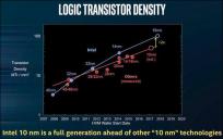
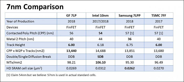
In is total mess with different tech names

Gwennap writes that the “7-nanometer” technology of TSM and Samsung and Global should be quite close to Intel’s 10-nanometer process, with the result that "the three leading foundries, which serve all of Intel’s major competitors, [will be] on the same level as the x86 giant."
Taiwan Semi’s 7-nano technology “appears similar to Intel’s 10nm, within a fraction of a node,” he writes. It’s even possible the three competitors will leap-frog Intel’s results before the chip giant can move to its next technology, sometime in 2021, writes Gwennap.
 sa2788.jpg622 x 390 - 39K
 -
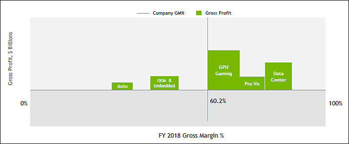
Nvidia rising development costs
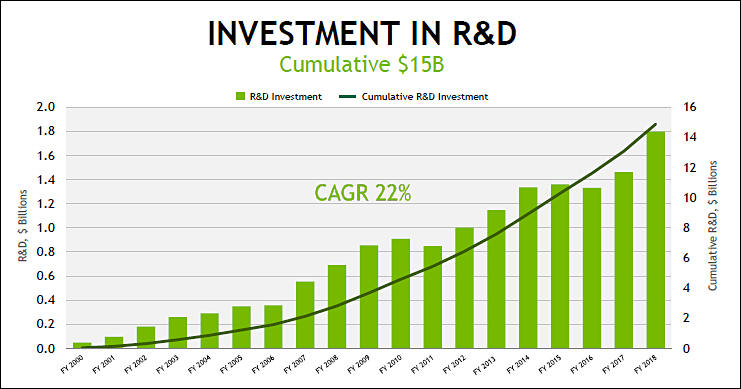
yet they have lot of margin left
 sa2437.jpg741 x 389 - 55K
 sa2438.jpg715 x 295 - 22K
 -
Very interesting information
Engineers see many options to create 5-, 3- and even 2-nm semiconductor process technologies, but some are not sure that they will be able to squeeze commercial advantages from them even at 5 nm.
Speed gains of 16% at 10 nm may dry up at 7 nm due to resistance in metal lines. Power savings will shrink from 30% at 10 nm to 10–25% at 7 nm, and area shrinks may decline from 37% at 10 nm to 20–30% at 7 nm, said Paul Penzes, a senior director of engineering on Qualcomm’s design technology team.
“Area still scales in strong double digits, but the hidden cost increases in masks means the actual cost advantages and other improvements are starting to slow down … It’s not clear what will remain at 5 nm,” said Penzes, suggesting that 5-nm nodes may only be extensions of 7 nm.
Versions of today’s FinFET transistors will be used down to the 5-nm node, said technologists from Synopsys and Samsung on the panel. Below a width of about 3.5 nm, FinFETs will hit a hard limit. Samsung has announced plans to use a gate-all-around transistor for a 4-nm process that it aims to have in production by 2020.
https://www.eetimes.com/document.asp?doc_id=1333109&page_number=1


Howdy, Stranger!
It looks like you're new here. If you want to get involved, click one of these buttons!
Categories
- Topics List23,993
- Blog5,725
- General and News1,354
- Hacks and Patches1,153
- ↳ Top Settings33
- ↳ Beginners256
- ↳ Archives402
- ↳ Hacks News and Development56
- Cameras2,368
- ↳ Panasonic995
- ↳ Canon118
- ↳ Sony156
- ↳ Nikon96
- ↳ Pentax and Samsung70
- ↳ Olympus and Fujifilm102
- ↳ Compacts and Camcorders300
- ↳ Smartphones for video97
- ↳ Pro Video Cameras191
- ↳ BlackMagic and other raw cameras116
- Skill1,960
- ↳ Business and distribution66
- ↳ Preparation, scripts and legal38
- ↳ Art149
- ↳ Import, Convert, Exporting291
- ↳ Editors191
- ↳ Effects and stunts115
- ↳ Color grading197
- ↳ Sound and Music280
- ↳ Lighting96
- ↳ Software and storage tips266
- Gear5,420
- ↳ Filters, Adapters, Matte boxes344
- ↳ Lenses1,582
- ↳ Follow focus and gears93
- ↳ Sound499
- ↳ Lighting gear314
- ↳ Camera movement230
- ↳ Gimbals and copters302
- ↳ Rigs and related stuff273
- ↳ Power solutions83
- ↳ Monitors and viewfinders340
- ↳ Tripods and fluid heads139
- ↳ Storage286
- ↳ Computers and studio gear560
- ↳ VR and 3D248
- Showcase1,859
- Marketplace2,834
- Offtopic1,320


