-
And even revised plan must be revised again and again
 sample904.jpg746 x 492 - 89K
 -
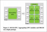
Nvidia is worried
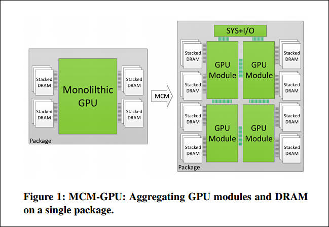
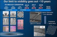
Unfortunately, despite the application performance scalability with the increasing number of SMs, the observed performance gains are unrealizable with a monolithic single-die GPU design. This is because the slowdown in transistor scaling eventually limits the number of SMs that can be integrated onto a given die area. Additionally, conventional photolithography technology limits the maximum possible reticle size and hence the maximum possible die size. For example, ≈ 800mm2 is expected to be the maximum possible die size that can be manufactured. For the purpose of this paper we assume that GPUs with greater than 128 SMs are not manufacturable on a monolithic die.
 sample804.jpg649 x 447 - 47K
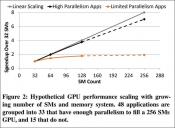 sample805.jpg800 x 584 - 81K
 -
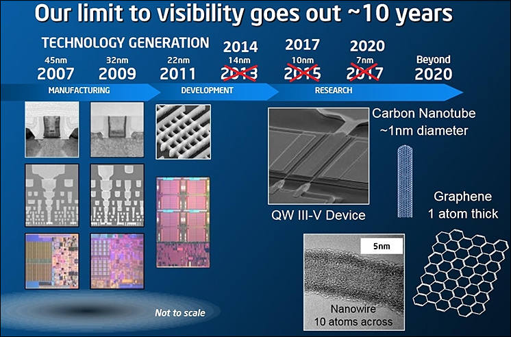
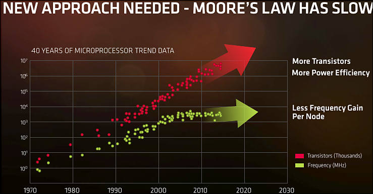
Transistors & The End of Moore's Law
-
IBMs 5nm tech
-
Optimism is fascinating:
TSMC disclosed previously its 7nm process will be ready for risk production in the second quarter of 2017, followed by volume production in 2018. The foundry has secured 12 design tape-outs for the process.
Samsung has unveiled plans to enter volume production of 7nm chips in 2018.
Globalfoundries recently announced the availability of its 7LP (7nm leading-performance) FinFET semiconductor technology, and expects the first customer products based on the technology to launch in the first half of 2018 with volume production ramping in the second half of 2018.
Of course things will shift a lot from this proposed data, at least for anything besides PGA and memory.
-
Intel forced to stay on 14nm for longer
And usual lie about 15% that will more like 0-3%
 sample357.jpg680 x 379 - 46K
 -
Optimism for investors
Taiwan Semiconductor Manufacturing Company (TSMC) is set to move its 7nm process technology to volume production in 2018, an improved version of the 7nm process using extreme ultraviolet (EUV) will be ready for volume production a year later, according to company co-CEO CC Wei.
TSMC's manufacturing technologies are offered to target four main applications - mobile, high-performance computing, automotive and IoT, Wei indicated. TSMC has already moved its 10nm process technology focusing mainly on mobile devices to volume production.
Now actually AMD could not meet demand due to simple fact that unable to produce enough 14nm chips.
Huge delays with 835 chip and total shortage of it also come from similar issue.
-
PR machine broke
Intel has evolved its event portfolio and decided to retire the IDF program moving forward. Thank you for nearly 20 great years with the Intel Developer Forum! Intel has a number of resources available on intel.com, including a Resource and Design Center with documentation, software, and tools for designers, engineers, and developers. As always, our customers, partners, and developers should reach out to their Intel representative with questions.
Intel cancelled both IDF events.
-
 sample1086.jpg750 x 977 - 154K
 -
Intel now propose that their 10nm is the real deal, else are all fakes


 sample1039.jpg678 x 388 - 40K
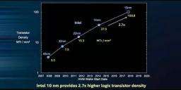 sample1040.jpg586 x 280 - 21K
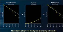 sample1041.jpg591 x 305 - 27K
 -
Yield rates for Taiwan Semiconductor Manufacturing Company's (TSMC) 10nm process technology have still been too low to boost the process to economies of scale, said the sources.
Yield rates for Samsung's 10nm process technology have been low affecting production for its own Exynos 8895 and Qualcomm's Snapdragon 835 chips, the sources revealed. The unsatisfactory 10nm yield rates have already pushed back Samsung's schedule to launch the next-generation Galaxy S8 smartphone.
-
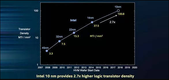
I don't understand this slide, supposedly showing the 3-year process advantage Intel has: http://images.anandtech.com/doci/11115/C4PU6KzWMAEglWH_575px.jpg
The 3-year gap they show is comparing Intel's 14nm process to competitors 10nm process. So is Intel saying that their 14nm process achieves higher density than the 10nm process from Samsung and others? And if so, how is this possible?
-
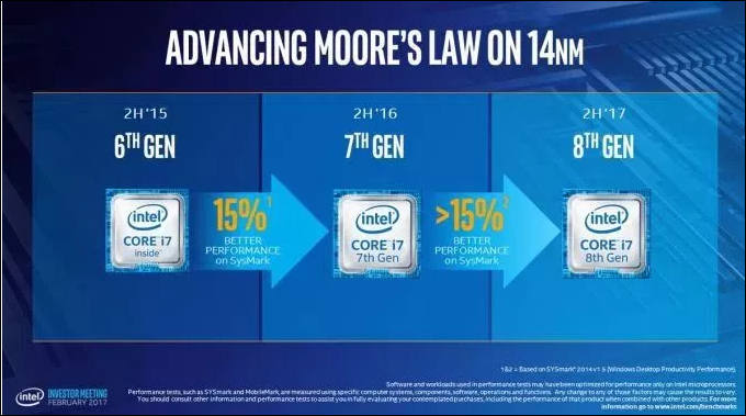
A quick news piece on information coming out of Intel’s annual Investor Day in California. As confirmed to Ashraf Eassa by Intel at the event, Intel’s 8th Generation Core microarchitecture will remain on the 14nm node. This is an interesting development with the recent launch of Intel’s 7th Generation Core products being touted as the ‘optimization’ behind the new ‘Process-Architecture-Optimization’ three-stage cadence that had replaced the old ‘tick-tock’ cadence. With Intel stringing out 14nm (or at least, an improved variant of 14nm as we’ve seen on 7th Gen) for another generation, it makes us wonder where exactly Intel can promise future performance or efficiency gains on the design unless they start implementing microarchitecture changes.
-
When a manufacturer converts from standard lithography to a double-patterning approach the lithography tool resolution is relaxed, and this shows on the chart’s top blue line. This line shows the lithography requirements for each process. A 45nm process uses 45nm lithography. Since 35nm uses double-patterning, then the lithography backs off to 70nm, and the 25nm process uses 50nm lithography. At 16nm, since quadruple patterning is used, lithography backs off to 4 x 16nm = 64nm.
SDAP limit is around 19nm btw
-
Intel sales dynamics

Number of sold CPU drop, prices rise. All as expected.
 sample414.jpg784 x 164 - 30K
 -
Both Taiwan Semiconductor Manufacturing Company's (TSMC) and Samsung's 10nm processes have reached lower-than-expected yield rates, according to industry sources. Yield rates for TSMC's 10nm process technology are not what the foundry expected, the sources said.
Yield rates for Samsung's 10nm process technology have been low prompting Qualcomm to turn cautious about its product roadmap for 2017, the sources said. Qualcomm originally planned for the Snapdragon 835 and other chips including the 660 (codenamed 8976 Plus) built using Samsung's 10nm process, but has revised its roadmap by having only the 835-series made using the newer node technology.
-
More details about marketing fluff called "silicon 4.0" mentioned above by eetimes
As for the future of semiconductor technology development, pitch shrinkage technology that has been adopted since the age of Silicon 1.0, is still widely used, but for 10nm, the transistor's shrinkage is actually only 14nm, while 7nm is actually 12nm, and 5nm is only 10nm. So now the semiconductor industry is about to enter the age of Silicon 4.0, said Lu, who added that he refers TSMC's four major growth areas - smartphone, high performance computing (HPC), Internet of Things (IoT) and car-use electronics, which will all be based on its smart semiconductor platform, are the applications targeted in age of Silicon 4.0.
-
As the global semiconductor industry moves into the 7nm process, there are only four companies that can offer related products, Globalfoundries, TSMC, Samsung and Intel, of which two are pure-play foundries. We value much the 7nm process believing that this process will be a very important and long-living technology for the semiconductor industry; we have already secured a number of clients and we have great confidence in the 7nm process race.
We decided to jump from 14nm to 7nm directly, while skipping the 10nm process because we believe that 10nm will help not much to improve power consumption and costs for clients; the 10nm node is more like a semi-generation process, similar to the previous the 20nm technology, which could not meet clients' requirements.
-
Samsung progress
Samsung Electronics is expanding its advanced foundry process technology offerings with the fourth-generation 14-nanometer (nm) process (14LPU) and the third-generation 10nm process (10LPU) to meet the requirements of next generation products ranging from mobile and consumer electronics to data centers and automotives.
Samsung presented these new technology offerings at the Samsung Foundry Forum to foundry customers and partners. The event was held at its Device Solutions America headquarters today, where the company elaborated on the details of new technology offerings including 14LPU and 10LPU.
Samsung’s fourth-generation 14nm process technology, 14LPU, delivers higher performance at the same power and design rules compared to its third-generation 14nm process (14LPC). 14LPU will be optimally suited for high-performance and compute-intensive applications.
-
There is evidence that linear scaling has already reached its physical limits. “People say they are doing 10nm process modes, but you will not find any line widths at that level,” Lu says.
That’s why technology development has gone non-linear. In 2011, Intel announced its Tri-gate technology, leading the way from planar development of transistors on silicon into three dimensions. With 3D, even scaling by a factor of 0.85 results in a transistor density that is more like 0.5 scaling in two dimensions, Lu says.
Other companies have followed that trend. Toshiba built 3D NAND in 48 layers, and that memory has been used in Apple’s iPhone 7. Samsung has taken the idea a step further with the creation of a 64-layer flash memory device. The technology level was only 32nm, yet it was the virtual equivalent of 13nm, Lu notes.
“Now we are in silicon age 2.0 with vertical transistors and a scaling parameter of 0.8 to 0.85,” Lu says. “Silicon 3.0 is like a 3D landscape. We are seeing more and more people going there.”
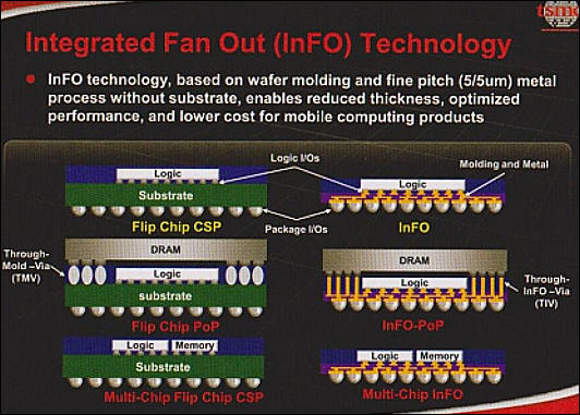
Lu says that his theory, as described in his paper, starts with Silicon 4.0. The advances from the current 3.0 generation have enabled a lot of new applications such as augmented reality, virtual reality and machine intelligence, he says. The next threshold is what Lu calls heterogeneous integration, or the incorporation of silicon and non-silicon materials by means of technologies such as integrated fan out (InFO).
http://www.eetimes.com/document.asp?doc_id=1330750
Note that flip chip shown on the left is widely used in cameras for long.
 img2826.jpg532 x 381 - 53K
 -
So it is official now
Qualcomm Incorporated (NASDAQ: QCOM) and NXP Semiconductors N.V. (NASDAQ: NXPI) today announced a definitive agreement, unanimously approved by the boards of directors of both companies, under which Qualcomm will acquire NXP. Pursuant to the agreement, a subsidiary of Qualcomm will commence a tender offer to acquire all of the issued and outstanding common shares of NXP for $110.00 per share in cash, representing a total enterprise value of approximately $47 billion.
https://www.qualcomm.com/news/releases/2016/10/27/qualcomm-acquire-nxp
-
Samsing 10nm PR
Following the successful mass production of the industry’s first FinFET mobile application processor (AP) in January, 2015, Samsung extends its leadership in delivering leading-edge process technology to the mass market with the latest offering.
“The industry’s first mass production of 10nm FinFET technology demonstrates our leadership in advanced process technology,” said Jong Shik Yoon, Executive Vice President, Head of Foundry Business at Samsung Electronics. “We will continue our efforts to innovate scaling technologies and provide differentiated total solutions to our customers.”
Samsung’s new 10nm FinFET process (10LPE) adopts an advanced 3D transistor structure with additional enhancements in both process technology and design enablement compared to its 14nm predecessor, allowing up to 30-percent increase in area efficiency with 27-percent higher performance or 40-percent lower power consumption. In order to overcome scaling limitations, cutting edge techniques such as triple-patterning to allow bi-directional routing are also used to retain design and routing flexibility from prior nodes.
The slower the progress - the more PR you need.
-
Who knows..
Google, Facebook, Amazon, IBM and Microsoft are joining forces to create a new AI partnership.


Howdy, Stranger!
It looks like you're new here. If you want to get involved, click one of these buttons!
Categories
- Topics List23,993
- Blog5,725
- General and News1,354
- Hacks and Patches1,153
- ↳ Top Settings33
- ↳ Beginners256
- ↳ Archives402
- ↳ Hacks News and Development56
- Cameras2,368
- ↳ Panasonic995
- ↳ Canon118
- ↳ Sony156
- ↳ Nikon96
- ↳ Pentax and Samsung70
- ↳ Olympus and Fujifilm102
- ↳ Compacts and Camcorders300
- ↳ Smartphones for video97
- ↳ Pro Video Cameras191
- ↳ BlackMagic and other raw cameras116
- Skill1,960
- ↳ Business and distribution66
- ↳ Preparation, scripts and legal38
- ↳ Art149
- ↳ Import, Convert, Exporting291
- ↳ Editors191
- ↳ Effects and stunts115
- ↳ Color grading197
- ↳ Sound and Music280
- ↳ Lighting96
- ↳ Software and storage tips266
- Gear5,420
- ↳ Filters, Adapters, Matte boxes344
- ↳ Lenses1,582
- ↳ Follow focus and gears93
- ↳ Sound499
- ↳ Lighting gear314
- ↳ Camera movement230
- ↳ Gimbals and copters302
- ↳ Rigs and related stuff273
- ↳ Power solutions83
- ↳ Monitors and viewfinders340
- ↳ Tripods and fluid heads139
- ↳ Storage286
- ↳ Computers and studio gear560
- ↳ VR and 3D248
- Showcase1,859
- Marketplace2,834
- Offtopic1,320


