-
AMD forgot to add that most progress is due to more cores :-)
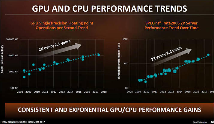
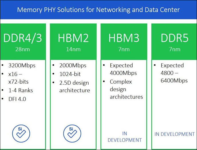
And here it is
AMD also said that they expect same size 7nm die CPU and GPUs to be twice more expensive.
 sa879.jpg714 x 416 - 56K
 sa880.jpg600 x 386 - 41K
 -
Intel will use cobalt in on the bottom two layers of its 10-nm interconnect to get a five- to ten-fold improvement in electromigration and a two-fold reduction in via resistance. It represents the first time that a chip maker has detailed plans to introduce cobalt — a brittle metal long considered a promising dielectric candidate — in a process, according to G. Dan Hutcheson.
Globalfoundries, which has said previously that it would insert EUV at the 7-nm node, detailed a platform that is entirely based on immersion optical lithography but is designed to enable the insertion of EUV for specific levels to improve cycle time and manufacturing efficiency. Gary Patton, Globalfoundries chief technology officer and senior vice president of global R&D, said in an interview with EE Times that kinks in EUV still need to be worked out — chiefly pellicle and inspection technologies — but that Globalfoundries is currently installing its first EUV production tools at its Fab 8 in upstate New York.
-
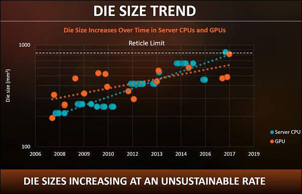
Many believe that the industry has slipped behind the pace of innovation prescribed by Moore's Law, which states the number of transistors per square inch of a chip would double every 18 months. Today, according to Su, it takes about 2.4 years to double the density of transistors per square inch. In addition, increasing die sizes are becoming economically problematic, memory bandwidth has become less efficient over time and the power consumption of SoCs is increasing by about 7 percent per year.
-
Serious issues with Intel 10nm process
To say yields were bad was understating things to a degree that even the classic British humorists would not dare to delve. Normally from tapeout to product on the shelves, Intel takes ~12 months for server SKUs, less for consumer. According to SemiAccurate moles, it has been ~16 months and counting.
Intel is insistent nothing is wrong but if you look at their recent Manufacturing Day messaging, one thing stood out. That thing is 20+ years of stating process progress was overturned with a new way of measuring progress that said that the 2+ year slip, at that time, for the 10nm process was not actually a problem, it was a technological breakthrough instead.
If you look at Intel roadmaps, the cadence should have gone 32nm (Westmere/Arrandale) in 2010, Sandy Bridge in 2011, Ivy Brige in 2012, Haswell in 2013, Broadwell in 2014, Sky Lake in 2015, Cannon Lake (10nm) in January 2016, Icelake (10nm) in January of 2017, and Tigerlake/Firelake (7nm) at CES in about 2 weeks aka January 2018. Instead there were the slips described above and Cannon, due ~2 years ago, isn’t out. Instead we have multiple “new architectures” that seem to pop up on the Intel roadmaps as soon as OEMs need to start production on the 10nm parts that were previously there.
10nm is now set for late 2018, officially, and that is where things really begin.
https://semiaccurate.com/2017/12/20/state-intels-10nm-process/
-
Intel issues are so serious that only 10nm CPUs they managed to make in 2017 are 2.2Ghz (in Turbo, normal is lower) 2 core one, without build in GPX. This allowed to make chip very small, so with horrible yields some can still work.
-
At CES 2018 Gregory Bryant told that high volume 10nm processor delivery to companies will start only in second half of 2018, may be closer to the end of year.
-
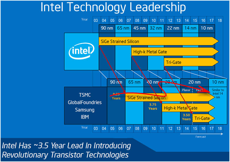
Some old but useful slide from Intel
-
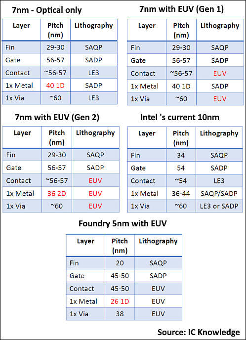
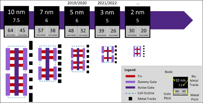
Interesting comparison of processes (it is prognosis for 2020 year processes)
-
UMC start cutting expenses for advanced processes (14nm an up).
Total capital expenses are also falling. In 2016 it was $2 billions, in 2017 it was only $1.44 billions and in 2018 it is planned to be only 1.1 billions
As predicted - each new step will require reduction in number of companies.
-
 sa1811.jpg419 x 244 - 36K
 -
5nm issues
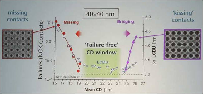
Researchers reported random defects appearing in extreme ultraviolet (EUV) lithography at 5-nm nodes. They are applying an array of techniques to eliminate them but, so far, see no clear solution.
A retired Intel lithographer predicted that engineers will be able to create 5-nm and even 3-nm devices by using two and three passes with an EUV stepper. But a rising tide of chip defects ultimately will drive engineers to new, fault-tolerant processor architectures such as neural networks, said Yan Borovodsky in a keynote at the event.
By 2024, defects could become so widespread that conventional processors will not be able to be made in leading-edge processes, said Borodovsky.
 sa2020.jpg650 x 302 - 31K
 sa2021.jpg543 x 667 - 90K
 -
Spending in 2017
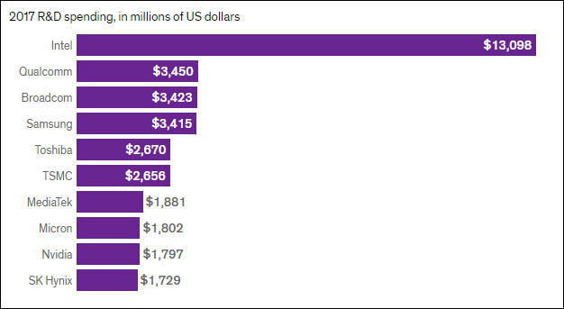
-
Very interesting information
Engineers see many options to create 5-, 3- and even 2-nm semiconductor process technologies, but some are not sure that they will be able to squeeze commercial advantages from them even at 5 nm.
Speed gains of 16% at 10 nm may dry up at 7 nm due to resistance in metal lines. Power savings will shrink from 30% at 10 nm to 10–25% at 7 nm, and area shrinks may decline from 37% at 10 nm to 20–30% at 7 nm, said Paul Penzes, a senior director of engineering on Qualcomm’s design technology team.
“Area still scales in strong double digits, but the hidden cost increases in masks means the actual cost advantages and other improvements are starting to slow down … It’s not clear what will remain at 5 nm,” said Penzes, suggesting that 5-nm nodes may only be extensions of 7 nm.
Versions of today’s FinFET transistors will be used down to the 5-nm node, said technologists from Synopsys and Samsung on the panel. Below a width of about 3.5 nm, FinFETs will hit a hard limit. Samsung has announced plans to use a gate-all-around transistor for a 4-nm process that it aims to have in production by 2020.
https://www.eetimes.com/document.asp?doc_id=1333109&page_number=1
-
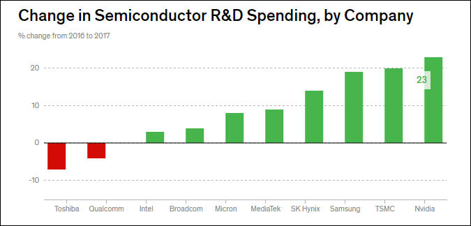
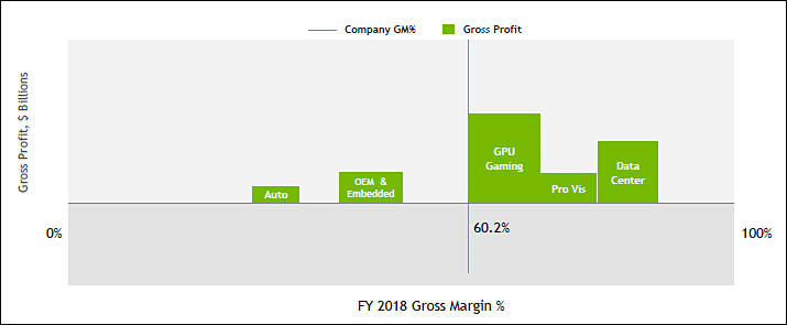
Nvidia rising development costs
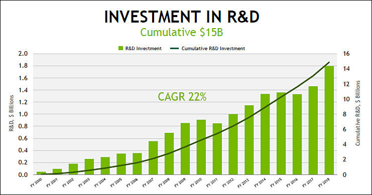
yet they have lot of margin left
 sa2437.jpg741 x 389 - 55K
 sa2438.jpg715 x 295 - 22K
 -
In is total mess with different tech names

Gwennap writes that the “7-nanometer” technology of TSM and Samsung and Global should be quite close to Intel’s 10-nanometer process, with the result that "the three leading foundries, which serve all of Intel’s major competitors, [will be] on the same level as the x86 giant."
Taiwan Semi’s 7-nano technology “appears similar to Intel’s 10nm, within a fraction of a node,” he writes. It’s even possible the three competitors will leap-frog Intel’s results before the chip giant can move to its next technology, sometime in 2021, writes Gwennap.
 sa2788.jpg622 x 390 - 39K
 -
James Prior from AMD - progress in CPU frequencies ended
-
No 10nm Intel chips until 2019 on the market
Problems continue.
We continue to make 14 nm process optimizations and architectural innovations in both data center and client products that will be coming this year.
Intel is currently shipping low-volume 10nm product and now expects 10nm volume production to shift to 2019.https://s21.q4cdn.com/600692695/files/doc_financials/2018/Q1/Q1-2018_EarningsRelease-FINAL.pdf
-
On JP Morgan conference Lisa Su told that things are not so bright with 7nm process.
Previously AMD shared only big optimism and now two staggering facts become known - new Vega 7nm will be small niche product aimed at miners and calculations and Zen2 architecture will come to Epyc very niche CPUs first. While Lisa Su carefully avoided it actually means that Ryzen 2 can be postponed to end of 2019 or even 2020.
-
Let's talk about the Company's sort of core leadership in manufacturing technology. I mean obviously Intel was the foundational architect of Moore's Law. The team has had a solid track record of driving performance, combination of you know your leadership in driving Moore's law and silicon process technology as well as architectural innovations as well. And you know just a little bit over a year ago at your Investor Day, the team described Intel being on track to scale logic scale area at a rate of 0.5x every two years, this is from a process technology perspective. Moreover at that event, you discuss Intel having an approximately three-year lead when versus competitors launching equivalent 10 nanometer processes.
Fast forward to today, Intel has delayed the high volume ramp of 10 nanometer, and with the leading foundry guys in the market bringing 7 nanometer products to the market maybe second half of this year arguably with similar sales and area type of benefits, as 10 nanometers, the markets getting a bit concerned that the gap is closing, and this potentially leads to the gap also closing between you and some of your competitors that take advantage of those process technology. So first off, could you just help us understand why Intel has made the decision to delay the 10 nanometer technology?
Murthy Renduchintala
Sure. Well and first of all, I think that silicon leadership is really important in as much as it supports product leadership. Silicon leadership in and of itself is only one of the aspects required. First of all Intel is a product company, it's not necessarily focused on being a merchant foundry. And in addition to silicon leadership, you really also need right architectural capability, the ability to execute silicon programs to predictable timelines, and you need an arsenal of capabilities and packaging, assembly and test technologies. So bringing all of those the weather is really what drives product leadership.
In terms of 10-nanometer, we are shipping 10-nanometer in low volumes. I think that if you go back to when we originally defined the recipe of 10-nanometer back in early 2014, we defined some very aggressive goals for our second-generation hyper-scaling. We targeted a 2.7x scaling factor, from 14-nanometers which was in the very stages of product ramp at that point in time. And 14-nanometers with in and of itself of 2.4x scaling on 22 nanometers, so clearly our engineering team in TMG had very, very ambitious goals in terms of the transistor scaling required.
That required a lot of innovations to come together and maybe those plans were a little bit more aggressive in hindsight than was ideal. And so, therefore we had a little bit of a greater challenge in bringing 10-nanometer to market than we had originally expected. However, the issues that we faced in getting that to prime time yield and not fundamental. We know what to fix and we’re busy going about fixing that. In the meantime, we found tremendous intra-node capability within our 14-nanometer process.
In fact from the very first generation of our 14-nanometer to the latest generation of 14-nanometer product, we've been able to deliver over 70% performance improvement as a result of those intra-node modifications and desirable changes. And that's quite frankly Harlan has given us the ability to make sure that we get 10-nanometer yields right before we go into mainstream production. And so, therefore we’re comfortable with the 14-nanometer roadmap that will give us leadership products in the next 12 to 18 months, as we seek to optimize the cost structure and yields of our 10-nanometer portfolio.
-
Samsung Process Technology Roadmap Updates
- 7LPP (7nm Low Power Plus): 7LPP, the first semiconductor process technology to use an EUV lithography solution, is scheduled to be ready for production in the second half of this year. Key IPs are under development, aiming to be completed by the first half of 2019.
- 5LPE (5nm Low Power Early): Through further smart innovation from the 7LPP process, 5LPE will allow greater area scaling and ultra-low power benefits.
- 4LPE/LPP (4nm Low Power Early/Plus): The use of highly mature and verified FinFET technology will be extended to the 4nm process. As the last generation of FinFET, 4nm provides a smaller cell size, improved performance, and faster ramp-up to the stable level of yield by adopting proven 5LPE, supporting easy migration.
- 3GAAE/GAAP (3nm Gate-All-Around Early/Plus): 3nm process nodes adopt GAA, the next-generation device architecture. To overcome the physical scaling and performance limitations of the FinFET architecture, Samsung is developing its unique GAA technology, MBCFET (Multi-Bridge-Channel FET) that uses a nano-sheet device. By enhancing the gate control, the performance of 3nm nodes will be significantly improved.
-
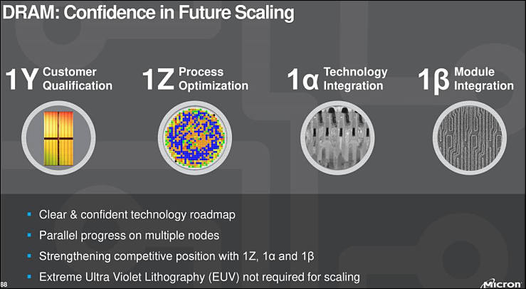
Micro thinks that EUV not required for DRAM scaling, for now at least
 sa3511.jpg739 x 406 - 47K
 -
TSMC moved its 7nm process dubbed N7 to volume production in the second quarter of 2018. The foundry expects sales generated from the node to account for over 20% in the fourth quarter of 2018 and 10% in all of the year. In addition to mobile devices, server CPU, network processors, gaming, GPU, FPGA, cryptocurrency, automotive and AI are the target applications of the N7.
An improved version of TSMC's N7 technology, dubbed N7 Plus, will adopt EUV lithography technology and become available in 2019, according to the foundry.
Wall hit will be very hard for industry it seems.
-
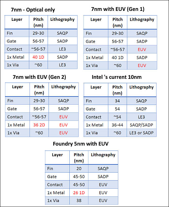
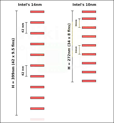
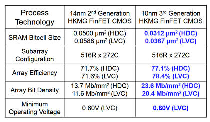
Details on Intel 10nm

- Logic transistor density of 100.8 mega transistors per mm2, increasing 10nm density 2.7X over the 14nm node
- Utilizes third generation FinFET technology
- Minimum gate pitch of Intel’s 10 nm process shrinks from 70 nm to 54 nm
- Minimum metal pitch shrinks from 52 nm to 36 nm
Process Highlights:
- Deepest scaled pitches of current 10 nm and upcoming 7 nm technologies
- First Co metallization and Ru usage in BEOL
- New self-aligned patterning schemes at contact and BEOL
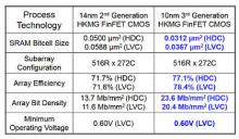
SRAM improvements
Moving contact to reduce footprint
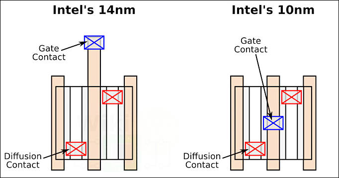
Metallization layers
 sa3616.jpg625 x 354 - 38K
 sa3617.jpg392 x 425 - 21K
 sa3618.jpg682 x 358 - 39K
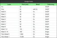 sa3619.jpg565 x 374 - 44K


Howdy, Stranger!
It looks like you're new here. If you want to get involved, click one of these buttons!
Categories
- Topics List23,991
- Blog5,725
- General and News1,354
- Hacks and Patches1,153
- ↳ Top Settings33
- ↳ Beginners256
- ↳ Archives402
- ↳ Hacks News and Development56
- Cameras2,367
- ↳ Panasonic995
- ↳ Canon118
- ↳ Sony156
- ↳ Nikon96
- ↳ Pentax and Samsung70
- ↳ Olympus and Fujifilm101
- ↳ Compacts and Camcorders300
- ↳ Smartphones for video97
- ↳ Pro Video Cameras191
- ↳ BlackMagic and other raw cameras116
- Skill1,960
- ↳ Business and distribution66
- ↳ Preparation, scripts and legal38
- ↳ Art149
- ↳ Import, Convert, Exporting291
- ↳ Editors191
- ↳ Effects and stunts115
- ↳ Color grading197
- ↳ Sound and Music280
- ↳ Lighting96
- ↳ Software and storage tips266
- Gear5,420
- ↳ Filters, Adapters, Matte boxes344
- ↳ Lenses1,582
- ↳ Follow focus and gears93
- ↳ Sound499
- ↳ Lighting gear314
- ↳ Camera movement230
- ↳ Gimbals and copters302
- ↳ Rigs and related stuff273
- ↳ Power solutions83
- ↳ Monitors and viewfinders340
- ↳ Tripods and fluid heads139
- ↳ Storage286
- ↳ Computers and studio gear560
- ↳ VR and 3D248
- Showcase1,859
- Marketplace2,834
- Offtopic1,319


