-
Samsung Electronics has revised its foundry process roadmap, skipping 4nm and jumping directly to 3nm from 5nm, according to industry sources.
Big issues at Samsung.
Also note that despite loud claims Samsung still do not make any significant amoung of complex chips using their 8nm process. Rumors are that both Apple and Nvidia tried to use it but failed.
-
TSMC R&D spending hit an all-time high of nearly US$3 billion last year.
TSMC disclosed in its annual report that R&D expenses grew about 4% on year to US$2.959 billion in 2019. The R&D spending accounted for 8.5% of the dedicated IC foundry's overall revenues last year, which came to a record high of NT$1.07 trillion.
TSMC also scaled up its R&D workforce to 6,534 employees in 2019, up 5% on year, according to the Taiwan-based foundry.
Sudden issues of TSMC can now mean full stop of all industry with unknown consequences.
-
Glogal ODM smartphone shipments are expected to reach 260 million units in 2020, down 41.6 million units or 13.5% from a year earlier, according to Digitimes Research.
Hard times coming for chipmakers.
-
TSMC will enter production using 5nm process technology later in June for Apple's custom-designed A14 processor and Qualcomm's Snapdragon X60 modem,
Rumors are that we can expect as much as 30% price hike for products made with 5nm TSMC process and around 20% for 7nm+ process (if they made it work finally).
Numeber of defective chips now is very high, hence TSMC even asked US to put sanctions on Huawei, as otherwise issues could become too public.
-
Supply chain partners of AMD, Nvidia and Intel have been left confused recently by the chip vendors' product launch schedules, which have either been changed frequently or kept a secret in their latest rounds of competition.
Issue with schedules is more related to TSMC and overall economcs situation.
It is now clear that something is up with so called TSMC 5nm process and that TSMC had been unablle to make 7nm+ process that uses EUV to work reliably still.
-
Another Intel top manager bites the dust
Intel announced that Jim Keller has resigned effective June 11, 2020, due to personal reasons. Intel appreciates Mr. Keller's work over the past two years helping them continue advancing Intel's product leadership and they wish him and his family all the best for the future. Intel is pleased to announce, however, that Mr. Keller has agreed to serve as a consultant for six months to assist with the transition.
Intel has a vastly experienced team of technical leaders within its Technology, Systems Architecture and Client Group (TSCG) under the leadership of Dr. Venkata (Murthy) Renduchintala, group president of TSCG and chief engineering officer. As part of this transition, the following leadership changes will be made, effective immediately:
-
Present data is that TSMC wants up to $25 billions USD from US goverment. This is size of special US fund for semiconductor productiona nd development. It is expected that TSMC and Intel will get up to 95% of this fund.
Without such taxpayer money semiconductor inductry can no longer develop, and it is only ont he approach to the hard wall.
-
TSMC is in talks with the US government about relevant subsidies for its new wafer fab in Arizona so that the foundry is able to implement the investment plan, said TSMC chairman Mark Liu at a press event right after the company's shareholders meeting on June 9.
Not only US taxpayer will pay for factory building. But they will also pay for each day of it working.
-
On why China still is pretty far from good position in this war
At the beginning of the semiconductor manufacturing process, monocrystalline silicon wafers are turned into chips. This procedure requires oxidation, coating, photolithography, etching, ion implantation, physical vapor deposition, chemical vapor deposition, polishing, wafer inspection and cleaning. Back-end processes include packaging and testing, backside thinning, wafer cutting, patching, wire bonding, molding, cutting tendon/forming, and final testing.
Semiconductor manufacturing equipment leading vendors
Oxidation/ RTP /laser annealing Applied Materials, Hitachi, Japan, Tokyo Electronics, Thermco, UK, Naura Technology Group Co., Beijing E-Town Semiconductor Technology
Glue development equipment
Tokyo Electronics, Deans, Germany SUSS, Austria EVG, Shenyang KingsemiLithography machines
ASML, Nikon Japan, Canon Japan, Tokyo Electronics, Applied Materials, Panlin Group, SEMES Korea, Shanghai Micro Electronics Equipment (Group) Co.Plasma etching machines
Pan Lin Group, Villian Semiconductor, Tokyo Electronics, Applied Materials, Hitachi, Japan JuSung, South Korea TES, AdvancedMicro-Fabrication Equipment Inc. China, North China ChuangIon implantation
Applied Materials, American Axcelies, German Ingun, American QA, American MicroXcat, Korean Leeno, Shanghai Kingstone Semiconductor, Beijing Zhongkexin Electronics Equipment, China Electronics Technology Group Corp.Physical vapor deposition
Applied Materials, Japan Evatec, Japan Ulvac, America Vaportech, Britain Teer, Switzerland Platit, Germany Cemecon, Beijing NMC Co., Sky Technology Development Co., Chengdu Rankuum Machinery, The 48th Research Institute of CETC, Cross-Tech Equipment Co.Chemical vapor deposition
Applied Materials, Panlin Group, American GT, Soitec, American ProtoFlex, French Semco, ASML, Tokyo Electronics, Nikon Japan, Canon Japan, North China Chuang, Shenyang Piotech Co.CMP equipment
Applied Materials, American Rtec, Japanese Evatec, HWatsing Technology, The 45th Research Institute of CETC, ACM ResearchWafer inspection: electrical inspection equipment, quality inspection equipment
Teradyne, Advantech, Tokyo Electronics, Corey Semiconductor, Applied Materials, Hitachi, Japan, Hangzhou Changchun Technology, Beijing Huafeng Test & Control Technology Co., Shanghai Zhongyi Automatic System Co., RISC Scientific Instrument (Shanghai) Co., Shanghai Jingce SemiconductorCleaning equipment
Japan Deans, Tokyo Electronics, Panlin Group, South Korea SEMES, North China Chuang, Shengmei Semiconductor, Pnc Process Systems Co., Shenzhen S.C. New Energy Technology Corp. -
And this is how the wall looks like
The American semiconductor industry is headed to Washington to push for $37 billion in federal funding to keep the industry competitive against China.
The SIA is asking for $5 billion in matched funding for a new semiconductor fab that would be operated in conjunction with a firm in the private sector — likely Intel. Intel CEO Bob Swan proposed in April that the company build a facility to work with the Pentagon on semiconductors for the defense sector. The SIA has earmarked a proposed $15 billion for states to provide incentives for the semiconductor industry to set up shop in their backyard, while the remaining $17 billion would be allocated for research and development funding.
As soon as smartphones sales no longer allow to move further firms look for the last option.
-
TSMC capital expenditures will be reduced
Due to the impact of Huawei’s new ban, some customers’ orders of TSMC (2330) were revised down, which led to a conservative view of the annual revenue. Capital expenditure in 2020 will be 13% lower than the company's previous forecast and 9% less than the previous year.
After negotiations with semiconductor equipment vendors, it was found that some new equipment orders for TSMC have been extended from June to December. The latest plan shows that the 5-nanometer process is likely to be reduced by 10,000 to 15,000 pieces per month compared to the previous plan, and the 7-nanometer process may be reduced by 10,000 to 20,000 pieces. The combined capital expenditure in 2020 and 2021 will be reduced by 5 to 7 billion US dollars .
And it is big issue for TSMC, especially if later we'll see second wave.
-
Some new idiotism
"TSMC's enhanced 5nm process enters mass production in Q4, ahead of schedule.
AMD's new Ryzen first to adopt. PC competitive landscape may usher in the biggest change in 15 years."
-
New AMD rumors
Present rumoprs are that APU Ryzen 6000 aka Rembrandt will use 6nm TSMC process.
It'll be slightly improved existing 7nm process with more EUV steps and little marketing adjustments.
Similar to fake 12nm AMD used before.
TSMC 5nm process is still very questionable and aimed at low power mobile chips.
3nm is just distant dreams for now.
Issue with 5nma dn 3nm considering CPU and GPU chips is that you no longer have enough surface to keep thermals good, as well as fact that with frequency rise transistor leaks become enormous.
-
SEMICONDUCTOR WAR UPDATE
Samsung is the top global producer of computer memory, smartphones and displays. Samsung is now spending $116 billion to compete with TSMC and Intel. They are building a cutting-edge chip production line south of Seoul – scheduled to start in the second half of 2021. Samsung will use extreme ultraviolet lithography to make chips for applications from 5G networks to ultra-high-performance computing.Samsung wants to take on Taiwan’s TSMC, producing for international clients. That will mean, essentially, China, with customers including Qualcomm.In parallel, Huawei bought a six-month supply of semiconductors from TSMC before the latest US sanctions. That will assure mid-term, but what matters is how China is catching up on semiconductors and chips at breakneck speed.That will require hundreds of thousands of engineers. And China, according to an Apple source, does have them. The source says that China has such massive engineering depth now that Apple itself can go NOWHERE ELSE to solve major engineering problems.This kind of depth in the US simply does not exist. US engineering schools have mostly foreign engineers. If some of them did not stay in the US, Exceptionalistan would be in deep trouble.This was confirmed to one of my sources by a top exec in a major, advanced US tech company: when he looks around the massive floor of engineers he supervises, no less than 2/3 are from China and India. -
GLOBALFOUNDRIES® (GF®), the world's leading specialty foundry and the leading U.S. pure-play manufacturer of semiconductors, today announced plans to implement export control security measures at its most advanced manufacturing facility, Fab 8, in Malta, New York. GF will bring its Fab 8 facility into compliance with both the U.S. International Traffic in Arms Regulations (ITAR) standards and the Export Administration Regulations (EAR), making the company the most advanced ITAR foundry in the country. By taking this significant step, GF deepens its partnership with the U.S. Department of Defense (DoD) and the U.S. defense industrial base, and further supports ongoing development of new assurance approaches in support of national security objectives.
These new control assurances, which will go into effect later this year, will make confidentiality and integrity protections available for defense-related applications, devices or components manufactured at GF’s Fab 8 facility. To date, GF has invested over $13 billion in Fab 8 and this is a significant step to serve the U.S. government and its technology needs for decades.
Senate Democratic Leader Chuck Schumer commented, “I have always been a strong believer that the most secure way to manufacture semiconductor chips is to do so here in the U.S. I have also been a champion of GLOBALFOUNDRIES and applaud their efforts to provide ITAR and EAR compliant manufacturing to the U.S. Government. In partnership with GF, New York State leads the nation in secure semiconductor manufacturing.”
Company can have US military as their main clients within 2 years.
TSMC story can also explain why all of the sudden GF dropped their own 7nm process and AMD had been ordered to use TSMC.
China goal now is to use any means, dirty tricks and open military force to destroy US - TSMC deal and also find weak spots in other US mased manufacturers logistics.
-
Got very interesting opinion today in talk
US goverment asked biggest bansk and funds for heavy investments in AMD 3-4 years ago as they need AMD during later stages of trade war. As well as same investments in TSMC.
US hoped that TSMC being largest manufacturer and AMD/Nvidia/Apple as biggest clients could help them avoid confrontaion with China and damage to US firms.
Recent Trump move can be actually aimed to fully destroy democratic party plan and largest California companies plans. Such way Trump goes into open confrontaion that can lead in few monst to horrible consequence for Apple, AMD and alike.
Chinese can move as far as block some of Taiwan exports to US.
-
Tragedy of TSMC
Taiwan Semiconductor Manufacturing Co., the world biggest contract chipmaker, has halted new orders from Huawei Technologies in response to tighter U.S. export controls aimed at further limiting the Chinese company's access to crucial chip supplies.
Huawei is TSMC's second-largest client only after Apple, accounting for 15-20% of its annual revenue. Huawei also accounted for up to 20% of SMIC's revenue, according to a Bernstein Research estimate.
According to the document posted online by the U.S. Commerce Department Bureau of Industry and Security, chip shipments bound for Huawei that went into production before May 15 and will ship before midnight Sept. 14 are not subject to the new rule. A license will be required for all other shipments.
Impact of this decision will be unprecidented.
It can be also only measure that could save Intel and buy 1-2 more years by keeping TSMC from moving forward.
-
TSMC today announced its intention to build and operate an advanced semiconductor fab in the US with the mutual understanding and commitment to support from the US federal government and the State of Arizona.
This facility, which will be built in Arizona, will utilize TSMC's 5nm technology for semiconductor wafer fabrication, have a 20,000 semiconductor wafer per month capacity, create over 1,600 high-tech professional jobs directly, and thousands of indirect jobs in the semiconductor ecosystem, the Taaiwan-based foundry house said.
Construction is planned to start in 2021 with production targeted to begin in 2024. TSMC's total spending on this project, including capital expenditure, will be approximately US$12 billion from 2021 to 2029. TSMC said this US facility not only enables the company to better support its customers and partners, it also provides foundry house with more opportunities to attract global talent. This project is of critical, strategic importance to a vibrant and competitive US semiconductor ecosystem that enables leading US companies to fabricate their cutting-edge semiconductor products within the US and benefit from the proximity of a world-class semiconductor foundry and ecosystem, TSMC said.
TSMC said it welcomes continued strong partnership with the US administration and the State of Arizona on this project, which will require significant capital and technology investments from TSMC. The company said the strong investment climate in the US, and its talented workforce make this and future investments in the US attractive to TSMC.
Board of directors changed opinion in 48 hours. As soon as real owners called.
-
TSMC and surprise strange news on US plant
Taiwan Semiconductor Manufacturing Co plans to build an advanced chip factory in Arizona. The plant would make 5-nanometer transistor chips for TSMC.
TSMC’s board made the decision to build the plant earlier this week at a meeting in Taiwan and may officially announced the plans as early as Friday.
The plans call for the factory to begin producing the chips by the end of 2023.
This fully contradicts all other reports.
But it can be special plot made by Apple and TSMC to explain low volume of 5nm production later this year and next year, as well as very big delays with further processes.
Something is happening with TSMC, as it lost around 30% of income in last months. Most probably we see now attempt of US to transfer newly printed money directly to most valuable asset they have.
-
Intel's fate
Wall Street semiconductor analysts have mixed feelings about the notion of Intel (ticker: INTC) jumping into the contract chip-making business in competition with Taiwan Semiconductor Manufacturing (TSM), which controls more than half of the global market,
Christopher Danely asserts in a research note Tuesday that a new Intel foundry would have a “very low chance of success.” On the one hand, he thinks the foundry market “is the only growth opportunity for Intel as it can leverage its technology leadership and experience in manufacturing.” He also notes that Taiwan Semi, also known as TSMC, operates with much higher operating margins than Intel.
The company is having issues with both seven- and 10-nanometer manufacturing lines.
Building a new, cutting-edge fab will take up to three years—and capital, between $10 billion and $20 billion. Intel has tried several times before to enter the foundry business, but hasn’t been successful,
Longer-term, Arya sees the possibility of Intel breaking up its design and manufacturing arms into separate companies.
This can happen as early as next year.
-
Hygon Dhyana (threadripper 1st gen sold to CHinese) will move to 7nm soon. Samsung or TSMC or both will make them.
Big danger here is that it won't AMD team who will do redesign for completely new process, but new team of more than 500 Chinese engineers.
AMD seems to make huge error providing all documentation and signing on terms where they can't stop it now.
CPU can jump to 32 cores even. But still will be using same mount.
Compatibility to older x399 chipset can be also in Chinese plans as they can sell them internationally in this case.
-
The foundry leader TSMC 5nm will enter the mass production phase in the third quarter. Although the main orders in the second half are still Apple and Huawei Hisilicon, including Qualcomm, MediaTek, Xilinx, Broadcom, Supermicro. In addition, the market has reported that Intel is expected to commission some of the 5nm chips by TSMC.
It is no sign of working 7nm process in Intel. Even 10nm still sucks badly.
With present issues in place we can have Intel leaving leading pack as soon as next year. Cancelling 7nm altogether similar to Showing results for GlobalFoundries.
-
Wall Street Journal sources say the White House is talking to Intel and TSMC about setting up US chip factories. While Intel already has a US presence, its discussions revolve creating a foundry that other companies could use for their products.
In the time of dangerous Chinese manufacturers rise (now only equipment control limit this rise) Wall Street Journal sources say the White House is talking to Intel and TSMC about setting up US chip factories. While Intel already has a US presence, its discussions revolve creating a foundry that other companies could use for their products.
This can actually put big stick in both TSMC and Intel front wheels, as they now will be forced to move best factories and make new ones in mostly in US, this means 3-4 years delay that can become fatal.
-
AMD feeling good
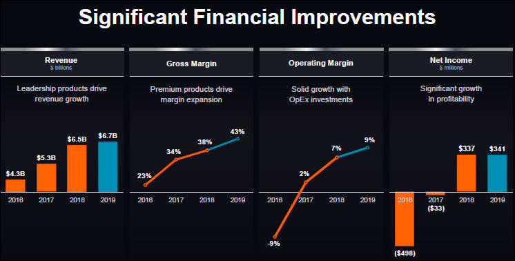
But due to issues with smartphones they will be forced to inject more in TSMC and marketing.
 sa12999.jpg746 x 378 - 51K
 -
Again on Moore law
Chiplets effectively bypass Moore's Law by replacing a single silicon die with multiple smaller dice that work together in a unified packaged solution. This approach provides much more silicon to add transistors compared to a monolithic microchip. As a result, chiplets are expected to allow a return to the two-year doubling cycle that has underpinned the economics of the semiconductor business since 1965.
"When semiconductor pioneer Gordon Moore first published his theory about semiconductor advancement, he provided a key forecasting benchmark that set a development cycle for the entire tech industry," said Tom Hackenberg, principal analyst, embedded processors, Omdia. "From software developers, to system designers, to tech investors, everyone for decades counted on the swift two-year schedule defined by Moore's Law. With the arrival of chiplets, the semiconductor business and those that depend upon it now have the opportunity to return to the customary rate of progress that has driven so much economic value for the overall tech industry."
Chiplets are experiencing adoption in more advanced and highly integrated semiconductor devices, i.e., microprocessors (MPU), system-on-chip (SoC) devices, graphics processing units (GPU) and programmable logic devices (PLD). The MPU segment represents the largest single market for chiplets among different microchip product types. The global market with chiplet-enabled MPUs is expected to expand to US$2.4 billion in 2024, up from US$452 million in 2018, according to Omdia.
"To remain competitive, MPU makers must always stick to the cutting edge of semiconductor manufacturing technologies," Hackenberg said. "These companies have the most to lose from the slowdown in Moore's Law. Because of this, these companies are among the earliest adopters of chiplets and are likely to be the primary contributors to chiplet standardization efforts."
MPU suppliers such as Intel and AMD are the early innovators building proprietary advanced packaging chiplets. Intel is also a member of the Open Compute Project, Open Domain-Specific Architecture (OCP ODSA) foundation, which is promoting the development of standards and technologies that are helping to enable advanced packaging strategies.
With the early adoption in MPUs, the computing segment is expected to be the dominant application market for chiplets through 2024, Omdia noted. Computing will account for 96% of revenue in 2020 and 92% by 2024.
Over the longer term, Omdia expects chiplet revenue to continue to expand and reach US$57 billion in revenue by 2035. Much of this growth will be driven by chiplets that serve as heterogenous processors, i.e., chips that combine different processing elements, such as applications processors that integrate graphics, security engines, artificial intelligence (AI) acceleration, low-power internet of things (IoT) controllers and more.
"Chiplets may not single-handedly save Moore's Law, but they do represent an innovative, emerging approach that help advance new packaging technologies, new design strategies and new materials," Hackenberg said. "This exciting new approach also may enable a more competitive landscape with diverse contributors. Chiplets will bolster the cadence Moore conveyed in his original 1965 article. The import of that original statement was not really about how microprocessors grow in performance. Rather, it was about establishing an industry guideline for a cadence that system designers, software developers and investors could count on to drive the innovation engine. This is the aspect of Moore's Law that will live on."
Too much hope for chiplets. They hope that issues with new processes could be hidden, no they won't.


Howdy, Stranger!
It looks like you're new here. If you want to get involved, click one of these buttons!
Categories
- Topics List23,993
- Blog5,725
- General and News1,354
- Hacks and Patches1,153
- ↳ Top Settings33
- ↳ Beginners256
- ↳ Archives402
- ↳ Hacks News and Development56
- Cameras2,368
- ↳ Panasonic995
- ↳ Canon118
- ↳ Sony156
- ↳ Nikon96
- ↳ Pentax and Samsung70
- ↳ Olympus and Fujifilm102
- ↳ Compacts and Camcorders300
- ↳ Smartphones for video97
- ↳ Pro Video Cameras191
- ↳ BlackMagic and other raw cameras116
- Skill1,960
- ↳ Business and distribution66
- ↳ Preparation, scripts and legal38
- ↳ Art149
- ↳ Import, Convert, Exporting291
- ↳ Editors191
- ↳ Effects and stunts115
- ↳ Color grading197
- ↳ Sound and Music280
- ↳ Lighting96
- ↳ Software and storage tips266
- Gear5,420
- ↳ Filters, Adapters, Matte boxes344
- ↳ Lenses1,582
- ↳ Follow focus and gears93
- ↳ Sound499
- ↳ Lighting gear314
- ↳ Camera movement230
- ↳ Gimbals and copters302
- ↳ Rigs and related stuff273
- ↳ Power solutions83
- ↳ Monitors and viewfinders340
- ↳ Tripods and fluid heads139
- ↳ Storage286
- ↳ Computers and studio gear560
- ↳ VR and 3D248
- Showcase1,859
- Marketplace2,834
- Offtopic1,320


