-
The semiconductor roadmap could extend a decade to a 1-nm node or it could falter before the 3-nm node for lack of new resist chemistries.
People now talk about disturbing uncertainties that are natural outgrowths of the many challenges perpetually appearing on the path to next-generation chip.
One of the next big challenges is brewing more sensitive resist materials for the 3-nm node. Today’s chemically amplified resists (CARs) “are OK for the current and maybe next generation, but we’d like new platforms,” said Tony Yen, a vice president at ASML.
The resists are one way to reduce random errors known as stochastics, an old problem but one raising its head aggressively as engineers push toward the 5-nm node. Yen was bullish that ASML will deal with the defects that threaten yields.
Phillipe Leray, a metrology specialist at imec, was less optimistic. “We have to tackle the defect challenge in the near future,” he said. “Time is running out, and I don’t see any solution around the corner.”
The challenges are so steep that engineers are widening the scope of solutions they are considering in every area of chip technology. “We are looking at just about everything in advanced patterning,” said consultant Erik Hosler, noting that EUV emerged from the advanced patterning section of the conference that he now helps oversee.
Moving to 450-mm wafers and 9-inch reticles is one of the few areas not worth pursuing given the cost and limited payback. “We had an extensive 450-mm effort years ago, but you need a whole ecosystem, and without it, we won’t drive that change,” said Rich Wise, a technology manager at Lam Research.
“We are making progress, but we can extrapolate to where features are less than the diameter of a silicon atom, so lithography-driven scaling will come to an end,” said Harry Levinson, a lithographer with AMD and GlobalFoundries for more than 30 years.
“Limits do exist, but the best way around them is to change the paradigm,” said Chris Mack, a veteran consultant and author on lithography. “The brick wall is often in our own minds — innovations can move it and then we repeat the process of pushing.”
Almost all will be talking about brick wall one year from now and in two years all main industries will hit it.
-
Intel develops their own 7nm process, but have even worse results than 10nm
 sa7232.jpg734 x 334 - 78K
 -
Industry rumors are that Samsung is talking to buy most GlobalFoundries assets. Same as I said before already.
-
Intel spent 29 billions in 2018 on 10nm and related things, this is up from around 12 billions that was enough during days of first 14nm chips.
And results are really disappointing, number of defective chips is still at 90-99%.
-
Intel 10nm mass production can be shifted further into 2020
Rumors started spreading that in the fall of 2019 we can see another false start of Intel 10nm process. Yields are still really horrible without any light in the tunnel ahead.
In the fall we can see release of 2-4 processors with really high prices to make supply volumes fit existing production. -
For five decades, there have been amazing improvements in the productivity and performance of integrated circuit technology. While the industry has surmounted many obstacles put in front of it, it seems the barriers keep getting bigger, IC Insights noted. Despite this, IC designers and manufacturers are developing solutions that seem more revolutionary than evolutionary to increase chip functionality.
TSMC's 5nm process is under development and scheduled to enter risk production in the first half of 2019, with volume production coming in 2020. The process will use EUV.
It'll be big wall, not barriers. Because as soon as real improvement will stop they won't be able to use usual practice or ramping up volume and/or price.
Already buyers of premium smartphones are mostly paying for slow progress we can observe. Intel also specially made price hike to try to inject more money (as it is only thing that current management understand).
-
200mm Wafer production rise as sign of issues

Start of trend on this curve exactly coincide with Intel 14 first issues and inability to move to 10nm fast.
Also everywhere in industry you can see old equipment being put back to work. As specialists do not expect any real progress soon.
 sa6990.jpg747 x 415 - 41K
 -
Industry new rumors
Despite the optimism about its 7nm chip sales, TSMC expressed caution about the foundry's overall operations citing factors on a macro level. The foundry expects 2019 to be "a slow year" for its business and also the global chip sector. It forecasts that the foundry segment will register only flat growth.
Small industry rumors leaks suggest that actual price for 7nm product is very high due to very low yields still. Issues with 7nm process can be real reason behind too big prices for iPhone and Samsung smartphones, as well as Radeon VII. In case of really lower prices they had no chances to supply the product.
-
TSMC 7nm process can actually have issues
Rumors are that costs of TSMC production is still pretty high and suitable for top smartphones only.
AMD new Radeon shortages are related to this.
Same as postponing new Ryzen release, industry rumors are that actual CPUs release will be divided by stages with only top price CPUs coming around September-October and most popular ones can be shifted up to December.
AMD mass market GPU Navi chips release will be also shifted to November-December on even to after 2020 CES.
-
Rumors are that we can hear some bad news during 2019 concerning 5nm process and such
Top investors are pulling out of industry. Mubadala Investment sold all AMD stock.
Now it become known that Vision Fund that belong to Softbank fully sold their $4 billion stocks package, even bearing some losses due to NVidea stock price drop.
2019 can be first year where all industry will hit the wall and will be faced with rising costs and fewer sales. -
Industry insiders tell that GlobalFoundries will be completely sold part by part to different manufacturers, their top assets can be bough by companies who still in this rat race.
-
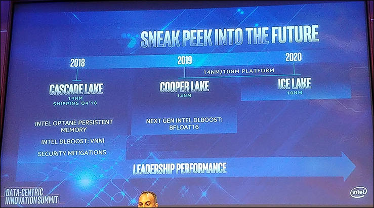
Intel still not fully sure if it can make 10nm in 2019
 sa6811.jpg719 x 257 - 117K
 -
 sa6515.jpg800 x 600 - 74K
 -
More on marketing
TSMC’s 7nm is not denser than Intel’s pending 10nm node. Intel’s 10nm process is actually denser than TSMC’s 7nm process – Intel's 10nm (6T) process is 100 mega-transistors per square millimeter (MTr/mm2), while TSMC's 7nm (7.5T) weighs in at 66 MTr/mm2.
-
AMD CTO about 7nm
“we had to literally double our efforts across foundry and design teams…It’s the toughest lift I’ve seen in a number of generations,” perhaps back to the introduction of copper interconnects, said Mark Papermaster.
Both AMD’s Zen 2 and Zen 3 x86 processors will be made in 7nm. “It’s a long node, like 28nm…and when you have a long node it lets the design team focus on micro-architecture and systems solutions” rather than redesign standard blocks for the next process
The technology is key for “an era of Moore’s law-plus where we’re getting new density advantages at each node and cost advantages as each new node matures, but mask costs are going up and chip frequencies are not going up, so how we put solutions together is critical to sustain the pace of development,” he said.
In software, “my call to action for the EDA community…is to redouble their efforts to take advantage of more CPU cores and parallelism…As the processing required for 7nm escalates…their algorithm optimization needs to take advantage of the very technology they are helping us manufacture,”
-
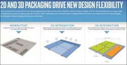
Intel 3D stacking tech, nothing new
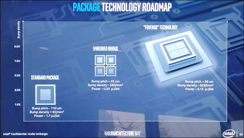

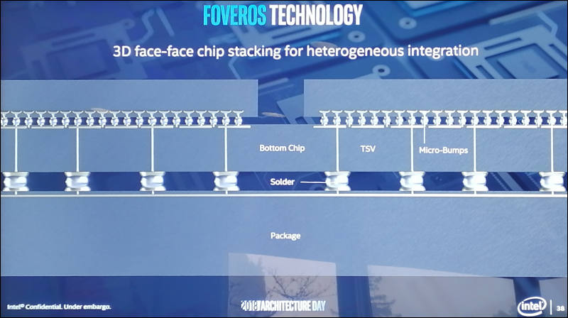
Note that it is badly suited for high performance chips due to cooling problems.
 sa6032.jpg796 x 406 - 66K
 sa6033.jpg800 x 452 - 55K
 sa6034.jpg800 x 448 - 58K
 sa6035.jpg800 x 448 - 55K
 -
More optimism before collapse into the wall
-
 sa5959.jpg791 x 411 - 52K
 sa5960.jpg792 x 411 - 71K
 -
3nm aka the wall aka final stop
Dr. Jung also introduced some of recent research and development in future silicon technology, including MRAM, a non-volatile memory solution embedded in conventional logic process, and 3nm Gate-All-Around (GAA) technology.
MRAM is one of the examples of new semiconductor devices that consume much less power. As memory density becomes higher, MRAM’s power efficiency becomes more prominent, consuming only 0.5% of power compared to SRAM at 1,024Mb. MRAM also has smaller cell area, which allows design flexibility.
Samsung’s unique GAA technology called Multi-Bridge-Channel FET(MBCFET) uses vertically stacked multiple nanosheet channels. With variable width of nanosheet, this technology provides not only optimal performance and power characteristics, but also high design flexibility. Furthermore, MBCFET is fabricated using 90% or more of FinFET process with only a few revised masks, allowing easy migration.
With one of its newly published papers at 2018 IEDM, Samsung Electronics shared the development progress of 3nm, a successful demonstration of fully functioning high-density SRAM circuit. The development of Samsung’s first process node applying MBCFET technology is on schedule.
-
Intel try to mitigate 10nm cancelling rumors. But already transfer some manufacturing areas back to 14nm.
Intel has no even definite plans for 7nm as had been told.
Main idea is same as for camera manufacturers - company just hiked prices.
 sa5338.jpg561 x 354 - 53K
 -
Just wow!
SemiAccurate has learned that Intel just pulled the plug on their struggling 10nm process. Before you jump to conclusions, we think this is both the right thing to do and a good thing for the company.
For several years now SemiAccurate has been saying the the 10nm process as proposed by Intel would never be financially viable. Now we are hearing from trusted moles that the process is indeed dead and that is a good thing for Intel, if they had continued along their current path the disaster would have been untenable. Our moles are saying the deed has finally been done.
Intel managers decline this
Media reports published today that Intel is ending work on the 10nm process are untrue. We are making good progress on 10nm. Yields are improving consistent with the timeline we shared during our last earnings report.
-
Intel own documents changes.
 sa4832.jpg706 x 515 - 100K
 sa4833.jpg739 x 411 - 65K
 -
Industry rumors are that Intel 10nm won't be usable for any 4 core or better CPUs for at least 2020.
Company has extreme problems with 10nm that they can't solve for many years.
-
In fact, 3nm and beyond may never happen at all, as there are a multitude of unknowns and challenges in the arena. Perhaps chip scaling will finally run out of steam by then.
At each node, process cost and complexity are skyrocketing, so now the cadence for a fully scaled node has extended from 18 months to 2.5 years or longer. In addition, fewer foundry customers can afford to move to advanced nodes.
One of the reasons here - capitalism, as everything is made under NDAs, buying and going around lot of patents. The more complex thing become - the more capitalism and it's son - copyright are holding progress.


Howdy, Stranger!
It looks like you're new here. If you want to get involved, click one of these buttons!
Categories
- Topics List23,983
- Blog5,725
- General and News1,353
- Hacks and Patches1,152
- ↳ Top Settings33
- ↳ Beginners255
- ↳ Archives402
- ↳ Hacks News and Development56
- Cameras2,362
- ↳ Panasonic992
- ↳ Canon118
- ↳ Sony156
- ↳ Nikon96
- ↳ Pentax and Samsung70
- ↳ Olympus and Fujifilm100
- ↳ Compacts and Camcorders300
- ↳ Smartphones for video97
- ↳ Pro Video Cameras191
- ↳ BlackMagic and other raw cameras115
- Skill1,960
- ↳ Business and distribution66
- ↳ Preparation, scripts and legal38
- ↳ Art149
- ↳ Import, Convert, Exporting291
- ↳ Editors191
- ↳ Effects and stunts115
- ↳ Color grading197
- ↳ Sound and Music280
- ↳ Lighting96
- ↳ Software and storage tips266
- Gear5,419
- ↳ Filters, Adapters, Matte boxes344
- ↳ Lenses1,582
- ↳ Follow focus and gears93
- ↳ Sound498
- ↳ Lighting gear314
- ↳ Camera movement230
- ↳ Gimbals and copters302
- ↳ Rigs and related stuff273
- ↳ Power solutions83
- ↳ Monitors and viewfinders340
- ↳ Tripods and fluid heads139
- ↳ Storage286
- ↳ Computers and studio gear560
- ↳ VR and 3D248
- Showcase1,859
- Marketplace2,834
- Offtopic1,319


