-
7nm progress
Taiwan Semiconductor Manufacturing Company (TSMC) has started commercial production of chips built using 7nm process technology.
TSMC will tape out more than 50 chip designs with its 7nm process technology by the end of 2018, Wei said. AI, GPU and cryptocurrency applications take up the majority of the tape-outs, followed by 5G and application processors.
TSMC will also start taping out chips built using an enhanced 7nm node with EUV in the second half of 2018.
5nm plans
TSMC's 5nm node's risk production is scheduled to kick off in the first half of 2019, with mass production at the end of the year or the beginning of 2020,
-
New tech to pack more stuff
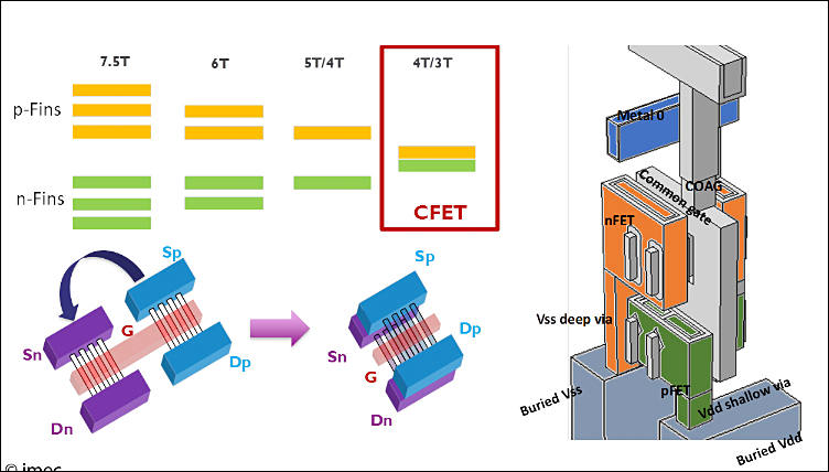
At this week’s 2018 Symposia on VLSI Technology and Circuits, imec, the world-leading research and innovation hub in nanoelectronics and digital technology, will present a process flow for a complementary FET (CFET) device for nodes beyond N3. The proposed CFET can eventually outperform FinFETs and meet the N3 requirements for power and performance. It offers a potential area scaling of both standard cells (SDC) and memory SRAM cells by 50%.
-
Problems now affect notebook vendors
Global notebook vendors including HP, Dell, Lenovo, Acer and Asustek Computer will be unable to launch new models fitted with Intel's new-generation CPUs in the second half of 2018 as scheduled, as the release of Intel's new offerings will not come soon enough for this year's high season
-
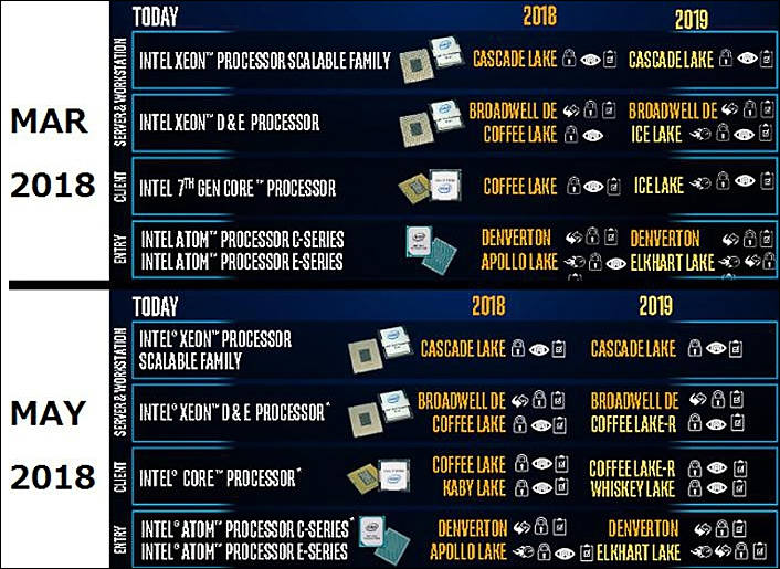
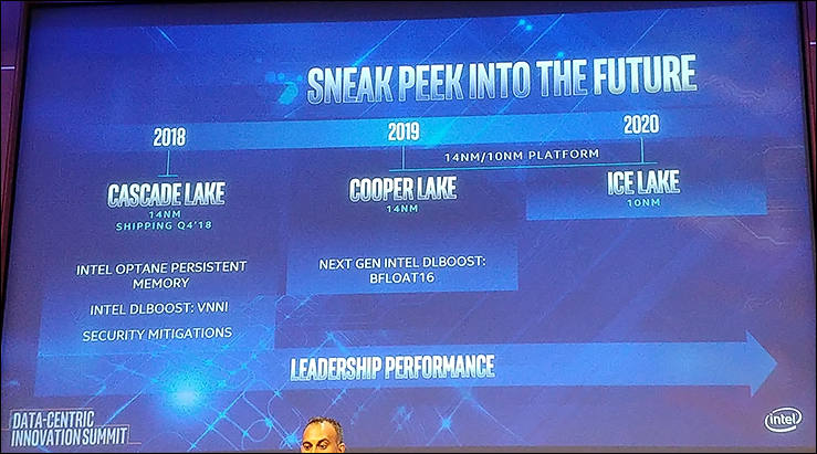
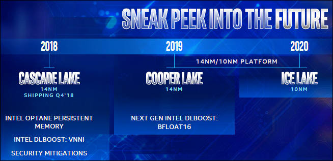
10nm Ice Lake based Xeon chips are postponed, They won't appear in 2019 and could be moved as far as 2021-22.
-
Intel expect no progress with 10nm until second half of 2019, at best
 sa3937.jpg735 x 428 - 107K
 -
Stop already happened for Intel and it'll go back
What Intel is not telling you, or the analysts, is that the 10nm you may get in late 2019 is not the 10nm they had intended to come out in 2015. More importantly this new process is a significant step backward from the 10nm they promised, as touted in their manufacturing day. How much of a step backwards? Several of SemiAccurate’s moles are saying it is effectively a 12nm process rather than a 10nm process, and the technical changes more than back that claim up.
https://semiaccurate.com/2018/08/02/intel-guts-10nm-to-get-it-out-the-door/
-
At 7mm we lost another player - GLOBALFOUNDRIES
GF is realigning its leading-edge FinFET roadmap to serve the next wave of clients that will adopt the technology in the coming years. The company will shift development resources to make its 14/12nm FinFET platform more relevant to these clients, delivering a range of innovative IP and features including RF, embedded memory, low power and more. To support this transition, GF is putting its 7nm FinFET program on hold indefinitely and restructuring its research and development teams to support its enhanced portfolio initiatives. This will require a workforce reduction, however a significant number of top technologists will be redeployed on 14/12nm FinFET derivatives and other differentiated offerings.
-
In perspective
Ten little Soldier Boys went out to dine;
One choked his little self and then there were nine.Nine little Soldier Boys sat up very late;
One overslept himself and then there were eight.Eight little Soldier Boys travelling in Devon;
One said he'd stay there and then there were seven.Seven little Soldier Boys chopping up sticks;
One chopped himself in halves and then there were six.Six little Soldier Boys playing with a hive;
A bumblebee stung one and then there were five.Five little Soldier Boys going in for law;
One got in Chancery and then there were four.Four little Soldier Boys going out to sea;
A red herring swallowed one and then there were three.Three little Soldier Boys walking in the zoo;
A big bear hugged one and then there were two.Two little Soldier Boys sitting in the sun;
One got frizzled up and then there was one .One little Soldier Boy left all alone;
He went out and hanged himself and then there were none. sa4464.jpg787 x 466 - 52K
 -
According to our sources, ATIC (Which owns about nine-tens of Globalfoundries) is in the process of looking for potential buyers for GlobalFoundries.
Nice.
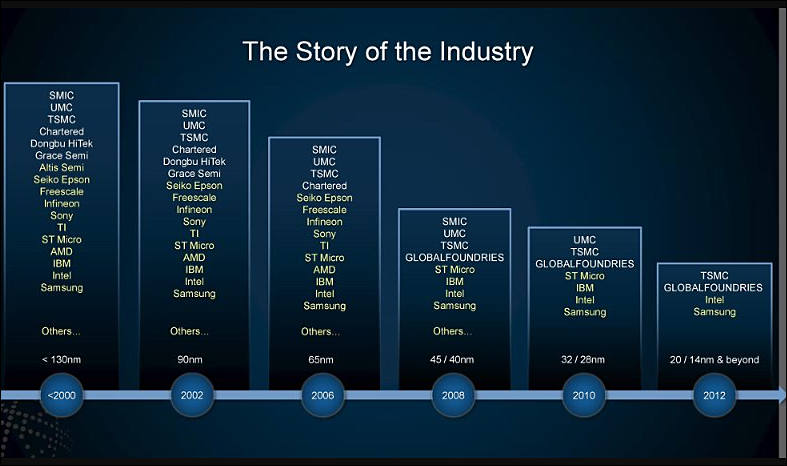
So from 4 remaining competitors:
- GlobalFoundries cancelled new technology, out of competition and will do 14nm and less only
- Intel has huge issues with 10nm (it is actually same or even better than others 7nm)
- TSMC use huge Apple money and seems to be on track for 7nm (yet not fully true 7nm)
- Samsung is similar to TSMC, but can also use their own big smartphones profits
-
In fact, 3nm and beyond may never happen at all, as there are a multitude of unknowns and challenges in the arena. Perhaps chip scaling will finally run out of steam by then.
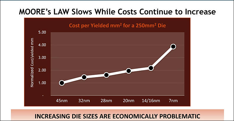
At each node, process cost and complexity are skyrocketing, so now the cadence for a fully scaled node has extended from 18 months to 2.5 years or longer. In addition, fewer foundry customers can afford to move to advanced nodes.
One of the reasons here - capitalism, as everything is made under NDAs, buying and going around lot of patents. The more complex thing become - the more capitalism and it's son - copyright are holding progress.
-
Industry rumors are that Intel 10nm won't be usable for any 4 core or better CPUs for at least 2020.
Company has extreme problems with 10nm that they can't solve for many years.
-
Intel own documents changes.
 sa4832.jpg706 x 515 - 100K
 sa4833.jpg739 x 411 - 65K
 -
Just wow!
SemiAccurate has learned that Intel just pulled the plug on their struggling 10nm process. Before you jump to conclusions, we think this is both the right thing to do and a good thing for the company.
For several years now SemiAccurate has been saying the the 10nm process as proposed by Intel would never be financially viable. Now we are hearing from trusted moles that the process is indeed dead and that is a good thing for Intel, if they had continued along their current path the disaster would have been untenable. Our moles are saying the deed has finally been done.
Intel managers decline this
Media reports published today that Intel is ending work on the 10nm process are untrue. We are making good progress on 10nm. Yields are improving consistent with the timeline we shared during our last earnings report.
-
Intel try to mitigate 10nm cancelling rumors. But already transfer some manufacturing areas back to 14nm.
Intel has no even definite plans for 7nm as had been told.
Main idea is same as for camera manufacturers - company just hiked prices.
 sa5338.jpg561 x 354 - 53K
 -
3nm aka the wall aka final stop
Dr. Jung also introduced some of recent research and development in future silicon technology, including MRAM, a non-volatile memory solution embedded in conventional logic process, and 3nm Gate-All-Around (GAA) technology.
MRAM is one of the examples of new semiconductor devices that consume much less power. As memory density becomes higher, MRAM’s power efficiency becomes more prominent, consuming only 0.5% of power compared to SRAM at 1,024Mb. MRAM also has smaller cell area, which allows design flexibility.
Samsung’s unique GAA technology called Multi-Bridge-Channel FET(MBCFET) uses vertically stacked multiple nanosheet channels. With variable width of nanosheet, this technology provides not only optimal performance and power characteristics, but also high design flexibility. Furthermore, MBCFET is fabricated using 90% or more of FinFET process with only a few revised masks, allowing easy migration.
With one of its newly published papers at 2018 IEDM, Samsung Electronics shared the development progress of 3nm, a successful demonstration of fully functioning high-density SRAM circuit. The development of Samsung’s first process node applying MBCFET technology is on schedule.
-
 sa5959.jpg791 x 411 - 52K
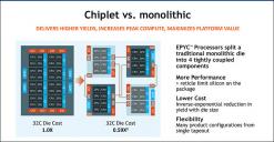 sa5960.jpg792 x 411 - 71K
 -
More optimism before collapse into the wall
-
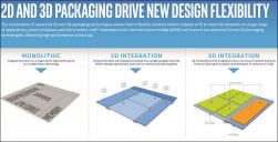
Intel 3D stacking tech, nothing new
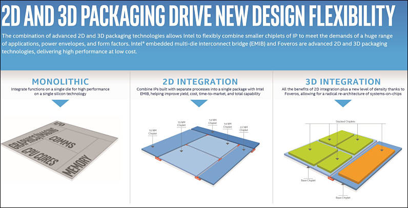
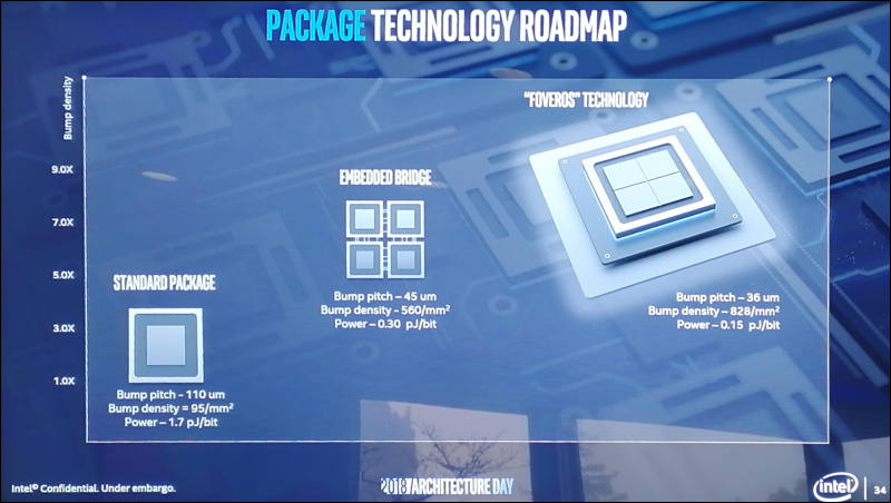

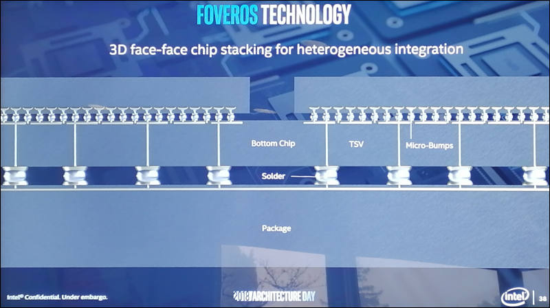
Note that it is badly suited for high performance chips due to cooling problems.
 sa6032.jpg796 x 406 - 66K
 sa6033.jpg800 x 452 - 55K
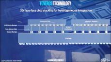 sa6034.jpg800 x 448 - 58K
 sa6035.jpg800 x 448 - 55K
 -
AMD CTO about 7nm
“we had to literally double our efforts across foundry and design teams…It’s the toughest lift I’ve seen in a number of generations,” perhaps back to the introduction of copper interconnects, said Mark Papermaster.
Both AMD’s Zen 2 and Zen 3 x86 processors will be made in 7nm. “It’s a long node, like 28nm…and when you have a long node it lets the design team focus on micro-architecture and systems solutions” rather than redesign standard blocks for the next process
The technology is key for “an era of Moore’s law-plus where we’re getting new density advantages at each node and cost advantages as each new node matures, but mask costs are going up and chip frequencies are not going up, so how we put solutions together is critical to sustain the pace of development,” he said.
In software, “my call to action for the EDA community…is to redouble their efforts to take advantage of more CPU cores and parallelism…As the processing required for 7nm escalates…their algorithm optimization needs to take advantage of the very technology they are helping us manufacture,”
-
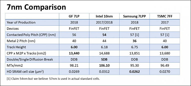
More on marketing
TSMC’s 7nm is not denser than Intel’s pending 10nm node. Intel’s 10nm process is actually denser than TSMC’s 7nm process – Intel's 10nm (6T) process is 100 mega-transistors per square millimeter (MTr/mm2), while TSMC's 7nm (7.5T) weighs in at 66 MTr/mm2.


Howdy, Stranger!
It looks like you're new here. If you want to get involved, click one of these buttons!
Categories
- Topics List23,990
- Blog5,725
- General and News1,353
- Hacks and Patches1,153
- ↳ Top Settings33
- ↳ Beginners256
- ↳ Archives402
- ↳ Hacks News and Development56
- Cameras2,366
- ↳ Panasonic995
- ↳ Canon118
- ↳ Sony156
- ↳ Nikon96
- ↳ Pentax and Samsung70
- ↳ Olympus and Fujifilm100
- ↳ Compacts and Camcorders300
- ↳ Smartphones for video97
- ↳ Pro Video Cameras191
- ↳ BlackMagic and other raw cameras116
- Skill1,960
- ↳ Business and distribution66
- ↳ Preparation, scripts and legal38
- ↳ Art149
- ↳ Import, Convert, Exporting291
- ↳ Editors191
- ↳ Effects and stunts115
- ↳ Color grading197
- ↳ Sound and Music280
- ↳ Lighting96
- ↳ Software and storage tips266
- Gear5,420
- ↳ Filters, Adapters, Matte boxes344
- ↳ Lenses1,582
- ↳ Follow focus and gears93
- ↳ Sound499
- ↳ Lighting gear314
- ↳ Camera movement230
- ↳ Gimbals and copters302
- ↳ Rigs and related stuff273
- ↳ Power solutions83
- ↳ Monitors and viewfinders340
- ↳ Tripods and fluid heads139
- ↳ Storage286
- ↳ Computers and studio gear560
- ↳ VR and 3D248
- Showcase1,859
- Marketplace2,834
- Offtopic1,320


