-
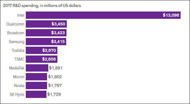
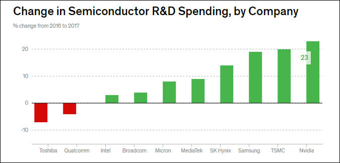
Spending in 2017
-
5nm issues
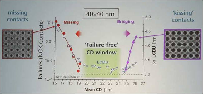
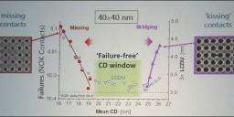
Researchers reported random defects appearing in extreme ultraviolet (EUV) lithography at 5-nm nodes. They are applying an array of techniques to eliminate them but, so far, see no clear solution.
A retired Intel lithographer predicted that engineers will be able to create 5-nm and even 3-nm devices by using two and three passes with an EUV stepper. But a rising tide of chip defects ultimately will drive engineers to new, fault-tolerant processor architectures such as neural networks, said Yan Borovodsky in a keynote at the event.
By 2024, defects could become so widespread that conventional processors will not be able to be made in leading-edge processes, said Borodovsky.
 sa2020.jpg650 x 302 - 31K
 sa2021.jpg543 x 667 - 90K
 -
 sa1811.jpg419 x 244 - 36K
 -
UMC start cutting expenses for advanced processes (14nm an up).
Total capital expenses are also falling. In 2016 it was $2 billions, in 2017 it was only $1.44 billions and in 2018 it is planned to be only 1.1 billions
As predicted - each new step will require reduction in number of companies.
-
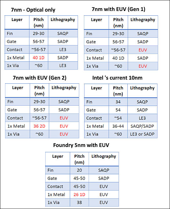
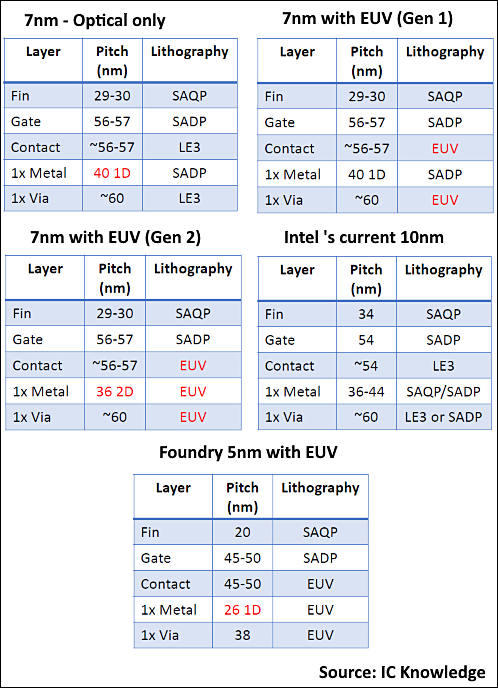
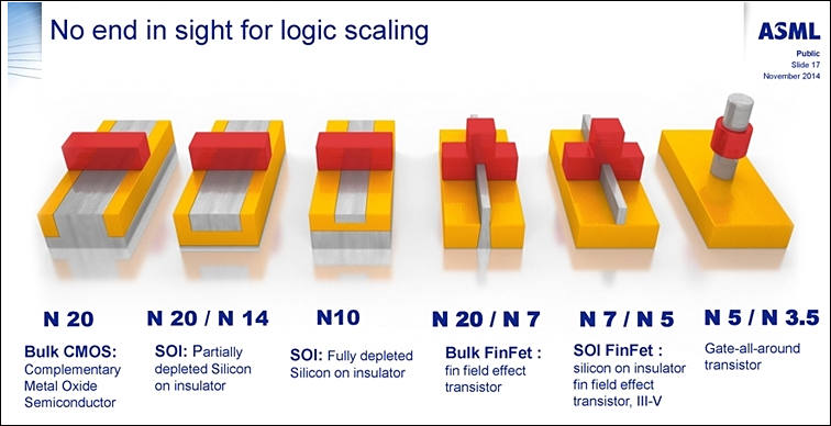
Interesting comparison of processes (it is prognosis for 2020 year processes)
-
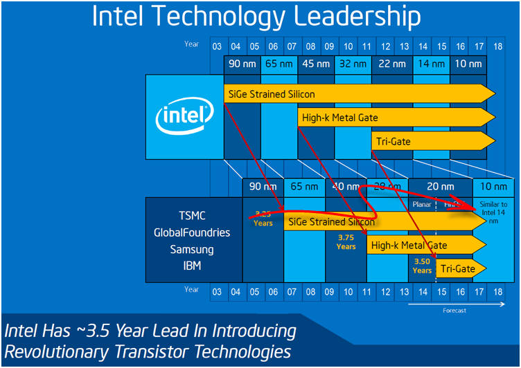
Some old but useful slide from Intel
-
At CES 2018 Gregory Bryant told that high volume 10nm processor delivery to companies will start only in second half of 2018, may be closer to the end of year.
-
Intel issues are so serious that only 10nm CPUs they managed to make in 2017 are 2.2Ghz (in Turbo, normal is lower) 2 core one, without build in GPX. This allowed to make chip very small, so with horrible yields some can still work.
-
Serious issues with Intel 10nm process
To say yields were bad was understating things to a degree that even the classic British humorists would not dare to delve. Normally from tapeout to product on the shelves, Intel takes ~12 months for server SKUs, less for consumer. According to SemiAccurate moles, it has been ~16 months and counting.
Intel is insistent nothing is wrong but if you look at their recent Manufacturing Day messaging, one thing stood out. That thing is 20+ years of stating process progress was overturned with a new way of measuring progress that said that the 2+ year slip, at that time, for the 10nm process was not actually a problem, it was a technological breakthrough instead.
If you look at Intel roadmaps, the cadence should have gone 32nm (Westmere/Arrandale) in 2010, Sandy Bridge in 2011, Ivy Brige in 2012, Haswell in 2013, Broadwell in 2014, Sky Lake in 2015, Cannon Lake (10nm) in January 2016, Icelake (10nm) in January of 2017, and Tigerlake/Firelake (7nm) at CES in about 2 weeks aka January 2018. Instead there were the slips described above and Cannon, due ~2 years ago, isn’t out. Instead we have multiple “new architectures” that seem to pop up on the Intel roadmaps as soon as OEMs need to start production on the 10nm parts that were previously there.
10nm is now set for late 2018, officially, and that is where things really begin.
https://semiaccurate.com/2017/12/20/state-intels-10nm-process/
-
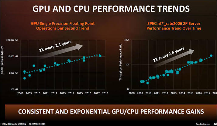
Many believe that the industry has slipped behind the pace of innovation prescribed by Moore's Law, which states the number of transistors per square inch of a chip would double every 18 months. Today, according to Su, it takes about 2.4 years to double the density of transistors per square inch. In addition, increasing die sizes are becoming economically problematic, memory bandwidth has become less efficient over time and the power consumption of SoCs is increasing by about 7 percent per year.
-
Intel will use cobalt in on the bottom two layers of its 10-nm interconnect to get a five- to ten-fold improvement in electromigration and a two-fold reduction in via resistance. It represents the first time that a chip maker has detailed plans to introduce cobalt — a brittle metal long considered a promising dielectric candidate — in a process, according to G. Dan Hutcheson.
Globalfoundries, which has said previously that it would insert EUV at the 7-nm node, detailed a platform that is entirely based on immersion optical lithography but is designed to enable the insertion of EUV for specific levels to improve cycle time and manufacturing efficiency. Gary Patton, Globalfoundries chief technology officer and senior vice president of global R&D, said in an interview with EE Times that kinks in EUV still need to be worked out — chiefly pellicle and inspection technologies — but that Globalfoundries is currently installing its first EUV production tools at its Fab 8 in upstate New York.
-
AMD forgot to add that most progress is due to more cores :-)
And here it is

AMD also said that they expect same size 7nm die CPU and GPUs to be twice more expensive.
 sa879.jpg714 x 416 - 56K
 sa880.jpg600 x 386 - 41K
 -
As it is too soon for 8nm, second gen 10nm is presented
Samsung announced that its Foundry Business has commenced mass production of System-on-Chip (SoC) products built on its second generation 10-nanometer (nm) FinFET process technology, 10LPP (Low Power Plus).
10LPP process technology allows up to 10-percent higher performance or 15-percent lower power consumption compared to its first generation 10nm process technology, 10LPE (Low Power Early). As this process is derived from the already proven 10LPE technology, it offers competitive advantages by greatly reducing turn-around time from development to mass production and by providing significantly higher initial manufacturing yield.
-
Samsung Electronics secured new customers from the U.S. and China for its 7-nano foundry business. This indicates that it succeeded in making a counterattack after it lost rights to produce Qualcomm’s 7-nano chips to TSMC. It is heard that it is finalizing a negotiation with Hwasung-si regarding construction of new 7-nano plant and finalize administrative procedures early December at the earliest. Positive forecast is seen for its 7-nano foundry business.
Qualcomm and Broadcom are designing next-generation chips through TSMC’s7-nano PDK. TSMC is planning to produce 7-nano chips by using normal steppers repeatedly. Due to this reason, many customers including Qualcomm decided to mass-produce their first 7-nano chips through TSMC.
It is expected that Samsung Electronics will be slightly late in commercializing 7-nano process than TSMC. However it has been emphasizing that its 7-nano process that is applied with EUV (Extreme Ultraviolet) photolithography technology is truly the next-generation process from all aspects such as area, performance, and amount of electricity consumption.
So, finally they are forced to do EUV.
-
Poor Moore law, they constantly want to dig up the grave and get out the corpse
The Moore's Law that sets the pace of the semiconductor development can last two more generations, as the process technology may hit bottlenecks after advancing to 3nm node from the existing 7nm and future 5nm nodes, Tsai Ming-kai, chairman of Taiwan's leading IC designer MediaTek, has said.
-
More surprises
Moore's Law has become invalid for a while, as the time needed for the transistor density to double is no longer 18-24 months, Morris Chang, chairman of Taiwan Semiconductor Manufacturing Company (TSMC) said.
TSMC will continue to increase transistor densities in the coming eight years, but will see a major challenge in 2025.
ASML CEO Peter Wennick said at the same forum that his company has worked out its technology development plans through 2030. It might be technologically feasible for ASML to carry out the plans, but the economic feasibility of the plans would meet with challenges before 2030.
-
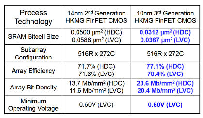
Intel and Globalfoundries will describe their 10nm and 7nm process nodes, respectively at the International Electron Devices Meeting (IEDM) in December. The event also will host papers pointing to new directions in memories, medical and flexible electronics and transistors beyond today’s FinFETs.
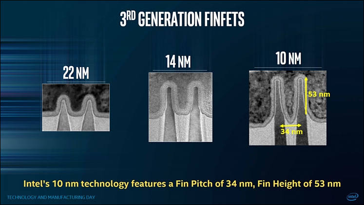
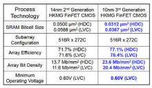
Intel will discuss several aspects of its 10nm node first unveiled in March. It sports FinFETs with a 7nm fin width at a 34nm pitch and a 46nm fin height made using self-aligned quadruple patterning. A 204 Mbit SRAM made in the process packs separate high-density, low voltage and high-performance cells that measure from 0.0312µm2 to 0.0441µm2.
 sa142.jpg747 x 421 - 44K
 sa143.jpg756 x 388 - 52K
 -
Samsung Electronics 8nm FinFET process
Samsung's new 8LPP process provides up to 10% lower power consumption with up to 10% area reduction from 10LPP through narrower metal pitch. 8LPP will provide differentiated benefits for applications including mobile, cryptocurrency and network/server, and is expected to be applied to many other high-performance applications, the company said.
"8LPP will have a fast ramp since it uses proven 10nm process technology while providing better performance and scalability than current 10nm-based products."
-
Intel afraid of EUV
A race is on to qualify advanced semiconductor process technologies using extreme ultraviolet (EUV) lithography, but Intel is said to be sitting on the sidelines.
Samsung and TSMC are racing to announce some level of manufacturing with EUV next year. But Intel is said not to be ordering materials needed for EUV at the same rate, according to one source that asked not to be named.
-
Still no EUV in DRAM
The industry was previously anticipated to transition to EUV litho technology beyond 20nm, but the high cost of EUV litho tools has discouraged Samsung and other DRAM chipmakers from pursuing the technology for their 1xnm manufacturing lines, said the sources. The DRAM industry will continue to stick with 193nm immersion lithography with multiple patterning for their 1ynm, and possibly 1znm lines for some of the players.
-
Nvidia founder and CEO Jensen Huang said that with the emergence of GPU computing following the decline of the CPU era, Moore's Law has come to an end. Huang made the statement when delivering a keynote speech at the GPU Technology Conference (GTC) China 2017, held on September 26 in Beijing.
Remarks came in sharp contrast to an earlier statement that Moore's Law will not fail, as issued by Intel at its Technology and Manufacturing Day held also in Beijing, on September 19, when the company provided updates for its 10nm process.
End for GPUs will be even harder and sharper.
-
EUV is last hope now

Firms and bosses did not wanted to use it, but now have no other option
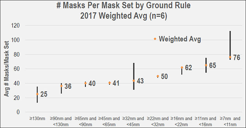
And this is why - masks count became too big.
 s841.jpg784 x 495 - 60K
 s842.jpg799 x 417 - 44K
 -
Intel Cannon Lake architecture will contain only small mobile CPUs.
Intel now is unable to produce 10nm big complex chips without very low yield rate.
Si it'll be around 2019 as you could see any 10nm desktop CPUs.


Howdy, Stranger!
It looks like you're new here. If you want to get involved, click one of these buttons!
Categories
- Topics List23,990
- Blog5,725
- General and News1,353
- Hacks and Patches1,153
- ↳ Top Settings33
- ↳ Beginners256
- ↳ Archives402
- ↳ Hacks News and Development56
- Cameras2,366
- ↳ Panasonic995
- ↳ Canon118
- ↳ Sony156
- ↳ Nikon96
- ↳ Pentax and Samsung70
- ↳ Olympus and Fujifilm100
- ↳ Compacts and Camcorders300
- ↳ Smartphones for video97
- ↳ Pro Video Cameras191
- ↳ BlackMagic and other raw cameras116
- Skill1,960
- ↳ Business and distribution66
- ↳ Preparation, scripts and legal38
- ↳ Art149
- ↳ Import, Convert, Exporting291
- ↳ Editors191
- ↳ Effects and stunts115
- ↳ Color grading197
- ↳ Sound and Music280
- ↳ Lighting96
- ↳ Software and storage tips266
- Gear5,420
- ↳ Filters, Adapters, Matte boxes344
- ↳ Lenses1,582
- ↳ Follow focus and gears93
- ↳ Sound499
- ↳ Lighting gear314
- ↳ Camera movement230
- ↳ Gimbals and copters302
- ↳ Rigs and related stuff273
- ↳ Power solutions83
- ↳ Monitors and viewfinders340
- ↳ Tripods and fluid heads139
- ↳ Storage286
- ↳ Computers and studio gear560
- ↳ VR and 3D248
- Showcase1,859
- Marketplace2,834
- Offtopic1,320


