It allows to keep PV going, with more focus towards AI, but keeping be one of the few truly independent places.
-
We present a systematic characterization of wafer-level reliability dedicated test structures in Back-Side-Illuminated CMOS Image Sensors. Noise and electrical measurements performed at different steps of the fabrication process flow, definitely demonstrate that the wafer flipping/bonding/thinning and VIA opening proper of the Back-Side-Illuminated configuration cause the creation of oxide donor-like border traps. Respect to conventional Front-Side-Illuminated CMOS Image Sensors, the presence of these traps causes degradation of the transistors electrical performance, altering the oxide electric field and shifting the flat-band voltage, and strongly degrades also reliability. Results from Time-Dependent Dielectric Breakdown and Negative Bias Temperature Instability measurements outline the impact of those border traps on the lifetime prediction.
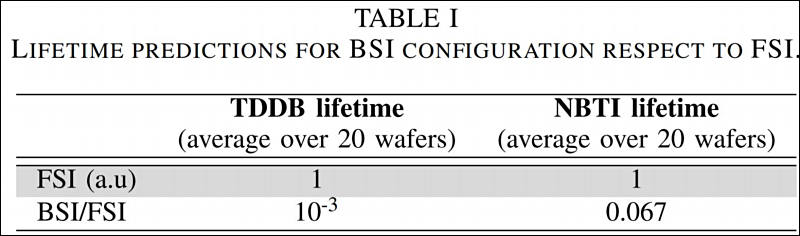
TDDB measurements were performed on n-channel Tx at 125C, applying a gate stress voltage Vstress in the range +7 to +7.6V. For each Vstress several samples were tested and the time-to-breakdown was measured adopting the three criteria defined in the JEDEC standard JESD92 [21]. For each stress condition, the fit of the Weibull distribution of the time-to-breakdown values gave the corresponding Time-to Failure (TTF). Then, the TTFs were plotted vs. Vstress in a log-log scale and the lifetime at the operating gate voltage was extrapolated with a power law (E-model [22]).
NBTI measurements were performed on p-channel Tx at 125C, applying Vstress in the range -3 to -4V. Again, several Tx were tested. Following the JEDEC standard JESD90, in this case, lifetime is defined as the stress time required to have a 10% shift of the nominal VT. The VT shift has a power law dependence on the stress time and the lifetime value at the operating gate voltage could be extrapolated.
We found that the donor-like border traps affect also the Back-Side device long term performance. Time Dependent Dielectric Breakdown and Negative Bias Temperature Instability measurements were performed to evaluate lifetime. As expected, the role of border traps in the lifetime prediction is different in the two cases, but the reliability degradation of Back-Side with respect to Front-Side-Illuminated CMOS Image Sensors is evident in any case.
https://ieeexplore.ieee.org/document/9060926
This can be especially important for new very dense 50-120Mp smartphones sensors.
 sa13511.jpg800 x 236 - 37K
 sa13512.jpg800 x 692 - 99K


Howdy, Stranger!
It looks like you're new here. If you want to get involved, click one of these buttons!
Categories
- Topics List23,984
- Blog5,725
- General and News1,353
- Hacks and Patches1,152
- ↳ Top Settings33
- ↳ Beginners255
- ↳ Archives402
- ↳ Hacks News and Development56
- Cameras2,363
- ↳ Panasonic993
- ↳ Canon118
- ↳ Sony156
- ↳ Nikon96
- ↳ Pentax and Samsung70
- ↳ Olympus and Fujifilm100
- ↳ Compacts and Camcorders300
- ↳ Smartphones for video97
- ↳ Pro Video Cameras191
- ↳ BlackMagic and other raw cameras115
- Skill1,960
- ↳ Business and distribution66
- ↳ Preparation, scripts and legal38
- ↳ Art149
- ↳ Import, Convert, Exporting291
- ↳ Editors191
- ↳ Effects and stunts115
- ↳ Color grading197
- ↳ Sound and Music280
- ↳ Lighting96
- ↳ Software and storage tips266
- Gear5,419
- ↳ Filters, Adapters, Matte boxes344
- ↳ Lenses1,582
- ↳ Follow focus and gears93
- ↳ Sound498
- ↳ Lighting gear314
- ↳ Camera movement230
- ↳ Gimbals and copters302
- ↳ Rigs and related stuff273
- ↳ Power solutions83
- ↳ Monitors and viewfinders340
- ↳ Tripods and fluid heads139
- ↳ Storage286
- ↳ Computers and studio gear560
- ↳ VR and 3D248
- Showcase1,859
- Marketplace2,834
- Offtopic1,319


