It allows to keep PV going, with more focus towards AI, but keeping be one of the few truly independent places.
-
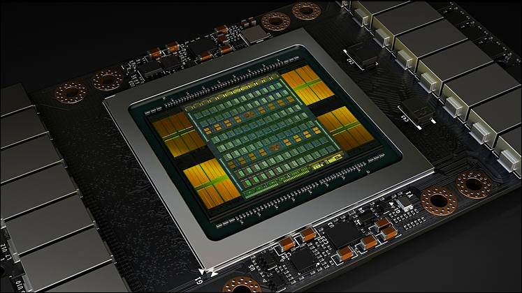
DECEMBER 17, 2018 – JEDEC Solid State Technology Association, the global leader in the development of standards for the microelectronics industry, today announced the publication of an update to JESD235 High Bandwidth Memory (HBM) DRAM standard. HBM DRAM is used in Graphics, High Performance Computing, Server, Networking and Client applications where peak bandwidth, bandwidth per watt, and capacity per area are valued metrics to a solution’s success in the market. The standard was developed and updated with support from leading GPU and CPU developers to extend the system bandwidth growth curve beyond levels supported by traditional discrete packaged memory. JESD235B is available for download from the JEDEC website.
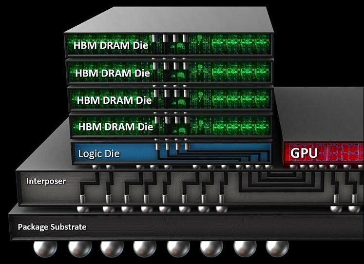
JEDEC standard JESD235B for HBM leverages Wide I/O and TSV technologies to support densities up to 24 GB per device at speeds up to 307 GB/s. This bandwidth is delivered across a 1024-bit wide device interface that is divided into 8 independent channels on each DRAM stack. The standard can support 2-high, 4-high, 8-high, and 12-high TSV stacks of DRAM at full bandwidth to allow systems flexibility on capacity requirements from 1 GB – 24 GB per stack.
This update extends the per pin bandwidth to 2.4 Gbps, adds a new footprint option to accommodate the 16 Gb-layer and 12-high configurations for higher density components, and updates the MISR polynomial options for these new configurations. Additional clarifications are provided throughout the document to address test features and compatibility across generations of HBM components.
 sa6121.jpg747 x 542 - 64K
 sa6122.jpg747 x 420 - 68K


Howdy, Stranger!
It looks like you're new here. If you want to get involved, click one of these buttons!
Categories
- Topics List23,990
- Blog5,725
- General and News1,353
- Hacks and Patches1,153
- ↳ Top Settings33
- ↳ Beginners256
- ↳ Archives402
- ↳ Hacks News and Development56
- Cameras2,366
- ↳ Panasonic995
- ↳ Canon118
- ↳ Sony156
- ↳ Nikon96
- ↳ Pentax and Samsung70
- ↳ Olympus and Fujifilm100
- ↳ Compacts and Camcorders300
- ↳ Smartphones for video97
- ↳ Pro Video Cameras191
- ↳ BlackMagic and other raw cameras116
- Skill1,960
- ↳ Business and distribution66
- ↳ Preparation, scripts and legal38
- ↳ Art149
- ↳ Import, Convert, Exporting291
- ↳ Editors191
- ↳ Effects and stunts115
- ↳ Color grading197
- ↳ Sound and Music280
- ↳ Lighting96
- ↳ Software and storage tips266
- Gear5,420
- ↳ Filters, Adapters, Matte boxes344
- ↳ Lenses1,582
- ↳ Follow focus and gears93
- ↳ Sound499
- ↳ Lighting gear314
- ↳ Camera movement230
- ↳ Gimbals and copters302
- ↳ Rigs and related stuff273
- ↳ Power solutions83
- ↳ Monitors and viewfinders340
- ↳ Tripods and fluid heads139
- ↳ Storage286
- ↳ Computers and studio gear560
- ↳ VR and 3D248
- Showcase1,859
- Marketplace2,834
- Offtopic1,320


